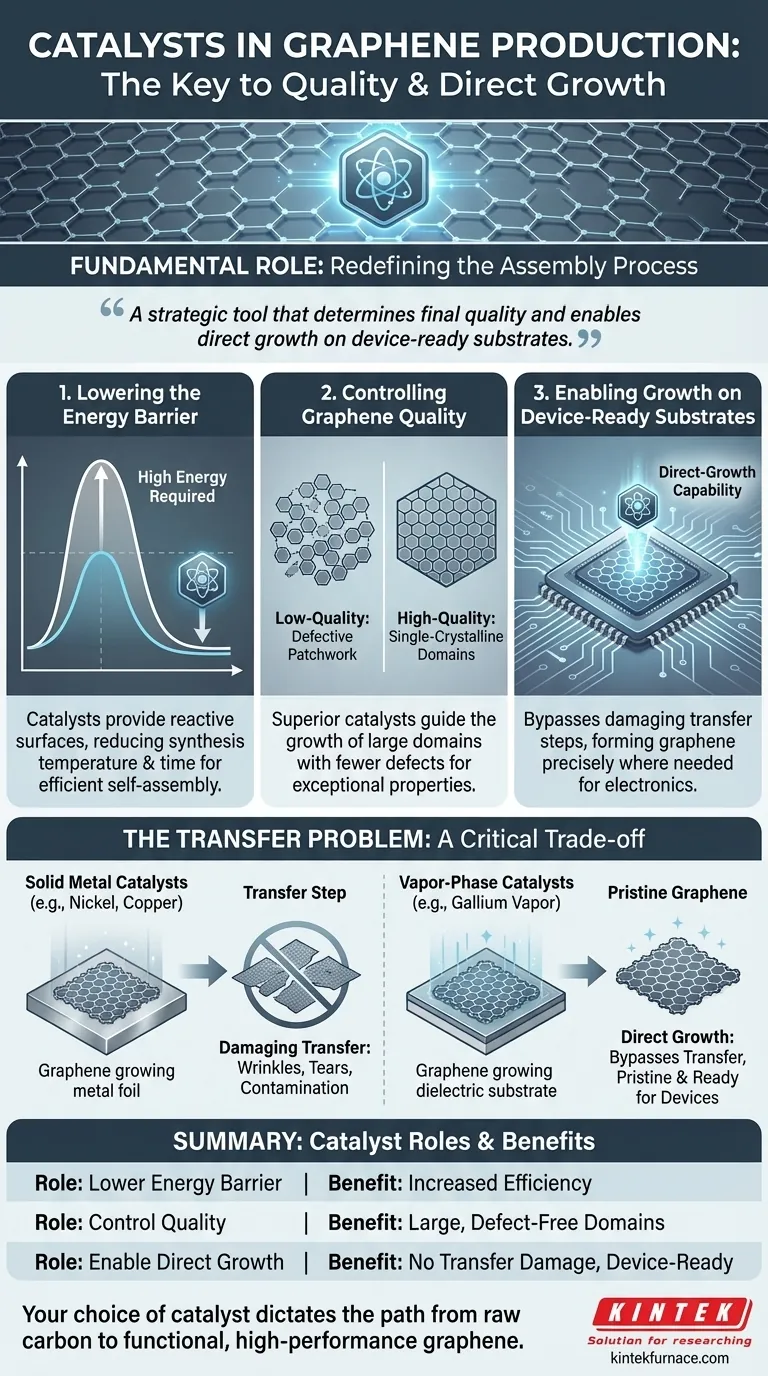
In graphene production, catalysts are essential substances that fundamentally alter the physical process of assembly. They dramatically lower the energy required to organize carbon atoms into a uniform, single-layer lattice and enable the growth of high-quality graphene directly on substrates that are useful for electronic devices.
The core role of a catalyst is not just to speed up graphene synthesis. It is a strategic tool that determines the final quality of the graphene and, most importantly, enables its direct growth on device-ready substrates, thus bypassing the damaging transfer steps that cripple its performance in high-end applications.
The Fundamental Role of Catalysts in Graphene Growth
To understand the importance of catalysts, we must first recognize the difficulty of forming perfect graphene. The process requires guiding individual carbon atoms into a flawless hexagonal honeycomb structure.
Lowering the Energy Barrier
Forming this perfect atomic lattice is an energetically demanding process. Catalysts provide a reactive surface or environment that makes it much easier for carbon precursor gases (like methane) to break down and for the resulting carbon atoms to self-assemble correctly.
This catalytic action significantly reduces the temperature and time needed for synthesis, making the entire process more efficient and viable.
Controlling Graphene Quality
The quality of a catalyst directly translates to the quality of the graphene. Superior catalysts guide the growth of large, single-crystalline domains.
A single-crystalline domain is a continuous area of the perfect hexagonal lattice with no breaks or misalignments. Larger domains mean fewer defects, which is absolutely critical for achieving the exceptional electronic and thermal conductivity graphene is known for.
Enabling Growth on Device-Ready Substrates
Perhaps the most critical role of modern catalysts is enabling the direct growth of graphene on dielectric substrates (insulators like silicon dioxide or sapphire).
Without a catalyst, growing graphene on these materials is nearly impossible. This direct-growth capability is a game-changer for electronics, as the graphene is formed precisely where it is needed for building transistors and other components.
Key Catalytic Methods and Their Implications
The choice of catalyst and its method of application dictates the properties of the final product and the complexity of the manufacturing process.
Solid Metal Catalysts (e.g., Nickel, Copper)
This is the most established method, where a thin foil of a metal like nickel or copper acts as the catalytic substrate. Graphene grows on the surface of the metal.
While effective for producing large sheets of graphene, this method has a significant drawback: the graphene must be physically transferred from the metal foil to the final device substrate.
Vapor-Phase Catalysts (e.g., Gallium Vapor)
In a more advanced technique known as gaseous catalyst-assisted Chemical Vapor Deposition (CVD), the catalyst exists as a vapor in the reaction chamber.
This method allows high-quality graphene to grow directly onto a separate, ultra-flat dielectric substrate. The catalyst facilitates the reaction without being permanently bonded to the substrate, neatly solving the transfer problem.
In-Situ Nanoparticles (e.g., Iron)
For some applications, catalysts like iron nanoparticles can be mixed directly with the carbon source. This "in-situ" method is often used to create graphene-based composites or powders where the graphene is embedded within a host material.
Understanding the Trade-offs: The Transfer Problem
The distinction between catalytic methods becomes clear when we examine the challenge of moving the finished graphene.
The Challenge of Solid Catalysts
When graphene is grown on a solid catalyst like nickel foam or copper foil, it is not on its final target. It must be painstakingly peeled off the metal and moved to a substrate like a silicon wafer.
The Damage of Transfer
This transfer process is the primary source of defects in mass-produced graphene. It almost invariably introduces wrinkles, tears, folds, and chemical contamination.
These imperfections severely degrade the graphene's electrical properties, hindering its use in high-performance electronics and optoelectronics.
Avoiding the Transfer Step
This is why methods like gaseous catalyst-assisted CVD are so valuable. By allowing graphene to grow directly on the final insulating substrate, they completely bypass the damaging transfer process. The result is pristine, high-performance graphene ready for device fabrication.
Making the Right Choice for Your Goal
Your application's requirements should guide your catalytic strategy. There is no single "best" method; only the most appropriate one for a specific objective.
- If your primary focus is high-performance electronics: Gaseous catalyst-assisted CVD is superior, as it produces transfer-free, high-quality graphene directly on dielectric substrates.
- If your primary focus is large-scale film production for less-sensitive applications: Traditional CVD on solid metal catalysts offers a mature and scalable method, but you must account for the performance loss from the transfer process.
- If your primary focus is creating graphene-based composites: In-situ catalysts like nanoparticles are effective for embedding graphene directly within other materials during synthesis.
Ultimately, your choice of catalyst directly dictates the path from raw carbon to functional, high-performance graphene.
Summary Table:
| Catalyst Role | Key Benefit | Common Methods |
|---|---|---|
| Lower Energy Barrier | Reduces synthesis temperature and time, increasing efficiency | Solid Metal (e.g., Nickel, Copper) |
| Control Quality | Enables large, single-crystalline domains with fewer defects | Vapor-Phase (e.g., Gallium Vapor) |
| Enable Direct Growth | Bypasses transfer step, preventing damage for high-performance electronics | In-Situ Nanoparticles (e.g., Iron) |
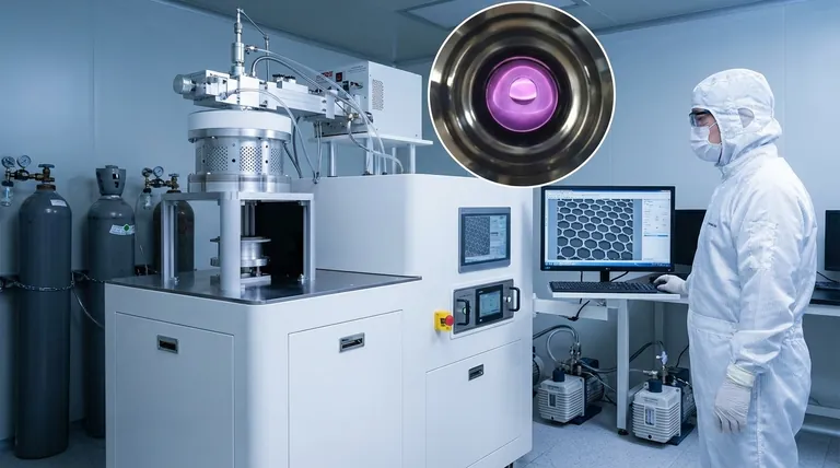
Ready to elevate your graphene production with tailored solutions? KINTEK leverages exceptional R&D and in-house manufacturing to provide advanced high-temperature furnace systems like Muffle, Tube, Rotary, Vacuum & Atmosphere Furnaces, and CVD/PECVD Systems. Our deep customization capabilities ensure precise alignment with your unique experimental needs, whether for electronics, composites, or large-scale films. Contact us today to discuss how we can optimize your catalyst processes and boost performance!
Visual Guide