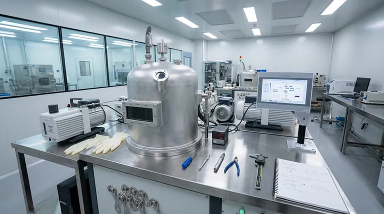
High-vacuum thermal evaporation coating equipment serves as the foundational tool for constructing the delicate vertical architecture of silicon quantum dot light-emitting diodes (SiQD LEDs). Its primary purpose is to deposit critical multilayer thin-film structures—specifically hole injection layers, electron transport layers, and metal electrodes—onto the device substrate with nanometer-scale precision.
By operating in an ultra-low pressure environment, this equipment enables the uniform deposition of functional materials while strictly preventing the oxidation of active layers, a requirement for ensuring efficient charge injection and long-term device stability.
Constructing the Device Architecture
Deposition of Carrier Transport Layers
The performance of a SiQD LED relies on how effectively it moves electrical charges. Thermal evaporation is used to deposit specific hole injection layers, such as Molybdenum Trioxide (MoO3), and electron transport layers.
These layers must be uniform to ensure that holes and electrons are injected efficiently into the quantum dots, allowing them to recombine and emit light.
Formation of Metal Electrodes
The equipment is also responsible for creating the electrical contacts of the device. It vaporizes and deposits metal electrodes, commonly composed of LiF/Al (Lithium Fluoride/Aluminum), Silver, or Gold.
Because these metals constitute the final electrical interface, their deposition must be controlled to prevent damage to the softer organic or quantum dot layers beneath them.
The Critical Role of the Vacuum Environment
Preventing Oxidation
The "high-vacuum" aspect is not merely a feature; it is a necessity. SiQD LEDs contain layers that are highly sensitive to oxygen and moisture.
Operating at ultra-low pressure eliminates atmospheric contaminants. This prevents the oxidation of the active layers during the coating process, which would otherwise degrade the device's brightness and lifespan.
Precision and Uniformity
In high-vacuum conditions, evaporated particles travel in straight lines with minimal scattering. This allows for precise management of layer thickness.
The equipment ensures uniform coverage and tight contact between the deposited layers and the underlying transport layers. This physical intimacy is vital for maximizing charge collection efficiency and minimizing electrical resistance.
Understanding the Operational Requirements
The Necessity of Rate Control
While thermal evaporation yields high-quality films, success depends on strictly managing the evaporation rate.
If the rate is too fast, the film may form unevenly or damage the underlying surface. If the rate is too slow, impurities from the chamber walls may incorporate into the film.
Sensitivity to Pressure Fluctuations
The process is intolerant of vacuum breaches. Even minor fluctuations in pressure can introduce oxygen into the chamber.
Consequently, the equipment requires robust pumping systems to maintain the deep vacuum necessary to guarantee the polarity adjustability and functional integrity of the final LED.
Optimizing Fabrication Results
To achieve the best performance from your SiQD LED fabrication process, consider these focal points:
- If your primary focus is Long-Term Stability: Prioritize the vacuum quality to prevent oxidation of the active layers during the deposition of the top electrode.
- If your primary focus is Charge Injection Efficiency: Ensure precise thickness control of the hole injection layer (e.g., MoO3) to facilitate optimal carrier transport.
Mastering the high-vacuum environment is the single most important step in transitioning from raw materials to a functioning, high-efficiency light-emitting device.
Summary Table:
| Component/Process | Purpose in SiQD LED Fabrication | Key Materials Used |
|---|---|---|
| Carrier Transport Layers | Facilitate hole and electron injection for light emission | MoO3, Organic Transport Materials |
| Metal Electrodes | Create electrical contacts and final interfaces | LiF/Al, Silver, Gold |
| High-Vacuum Environment | Prevents oxidation and ensures material purity | N/A (Process Condition) |
| Rate Control | Ensures film uniformity and prevents layer damage | N/A (Process Parameter) |
Elevate Your SiQD LED Research with KINTEK Precision
High-efficiency light-emitting devices demand uncompromising vacuum quality and nanometer-scale precision. KINTEK provides industry-leading high-vacuum thermal evaporation systems designed specifically for the delicate fabrication of quantum dot architectures.
Backed by expert R&D and manufacturing, KINTEK offers a full suite of Muffle, Tube, Rotary, Vacuum, and CVD systems, all customizable to meet your unique laboratory requirements. Whether you are optimizing charge injection or enhancing long-term device stability, our equipment ensures the uniformity and purity your materials deserve.
Ready to achieve superior coating results? Contact KINTEK today to discuss your custom solution.
References
- Ken‐ichi Saitow. Bright silicon quantum dot synthesis and LED design: insights into size–ligand–property relationships from slow- and fast-band engineering. DOI: 10.1093/bulcsj/uoad002
This article is also based on technical information from Kintek Furnace Knowledge Base .
Related Products
- HFCVD Machine System Equipment for Drawing Die Nano Diamond Coating
- Vacuum Hot Press Furnace Machine for Lamination and Heating
- 2200 ℃ Tungsten Vacuum Heat Treat and Sintering Furnace
- Multi Heating Zones CVD Tube Furnace Machine for Chemical Vapor Deposition Equipment
- Molybdenum Vacuum Heat Treat Furnace
People Also Ask
- What is Hot-filament Chemical Vapor Deposition (HFCVD)? Achieve High-Quality Thin Films with Precision Control
- What is the advantage of using a CVD system for coating turbine blades? Master Complex Geometries with Ease
- What materials are commonly used in CVD coating systems? Explore Key Materials for Superior Coatings
- What are the equipment for chemical vapor deposition? A Guide to the 5 Essential Components
- What is the function of high-purity Argon (Ar) gas during CVD? Optimize Your Thin Film Uniformity and Purity


