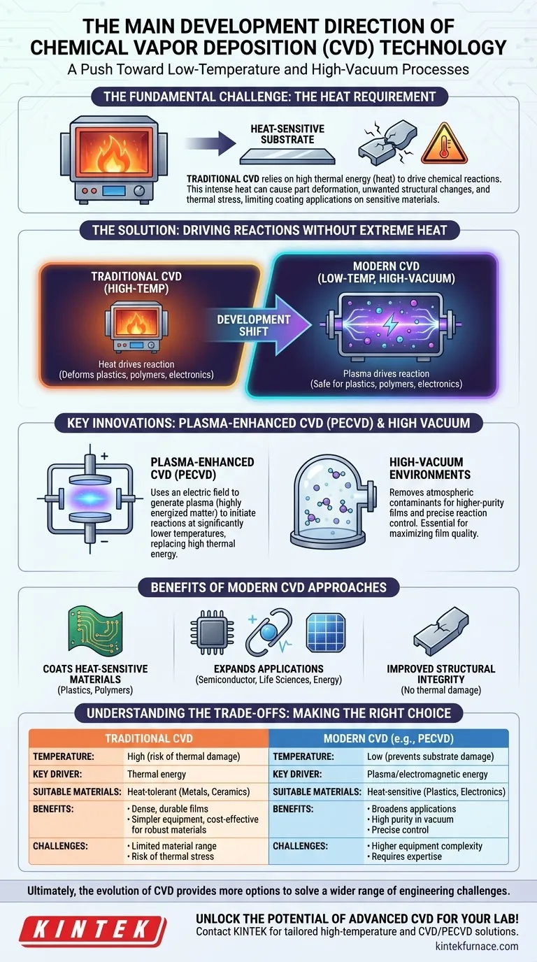
At its core, the primary development direction for improving Chemical Vapor Deposition (CVD) technology is the push toward low-temperature and high-vacuum processes. This strategic shift aims to overcome the significant limitations of traditional high-temperature methods, enabling the application of high-performance coatings on a much wider range of materials without causing thermal damage.
The fundamental challenge of CVD is that the heat required to drive the coating reaction can also damage the very part you're trying to protect. Therefore, the industry's main goal is to find new ways to energize this chemical reaction without relying on extreme, destructive temperatures.
The Fundamental Challenge of CVD: The Heat Requirement
Traditional CVD is a powerful process for creating durable, protective thin films. However, its reliance on high heat creates a significant engineering problem.
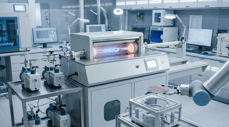
How Traditional CVD Works
The CVD process unfolds in four key stages: a precursor gas diffuses to the substrate, it's adsorbed onto the surface, a chemical reaction forms the solid film, and gaseous by-products are removed.
In conventional CVD, thermal energy is the engine that drives this critical chemical reaction. The entire chamber is heated to temperatures high enough to break down the precursor gases and deposit the desired film.
The Problem with High Temperatures
This reliance on extreme heat is the technology's primary drawback. High deposition temperatures can cause part deformation, unwanted structural changes, and thermal stress in the substrate material.
These effects can compromise the material's mechanical properties and weaken the bond between the coating and the surface. Critically, it also limits the types of materials that can be coated, excluding most plastics, polymers, and sensitive electronic components that cannot withstand the heat.
The Solution: Driving Reactions Without Extreme Heat
To broaden the applications of CVD, researchers and engineers are focused on developing methods that achieve the same high-quality coatings without the damaging side effects of intense heat.
The Goal: Low-Temperature, High-Vacuum
The central objective is to lower the deposition temperature. This allows for the coating of heat-sensitive materials and ensures the structural integrity of the finished part.
Operating in a high-vacuum environment is a complementary goal. A vacuum removes unwanted atmospheric molecules, preventing contamination and giving engineers precise control over the chemical reactions, leading to higher-purity films.
How Lower Temperatures Are Achieved
The most prominent solution is the use of plasma-assisted processes, often called Plasma-Enhanced CVD (PECVD).
Instead of relying solely on heat, PECVD uses an electric field to generate a plasma—a highly energized state of matter. This plasma provides the necessary energy to initiate the chemical reaction at a much lower temperature, effectively replacing thermal energy with electromagnetic energy.
Benefits of Modern CVD Approaches
By successfully lowering the process temperature, modern CVD methods unlock several key advantages. They enable the deposition of protective and functional coatings on plastics, complex electronics, and other sensitive substrates.
This expands the use of CVD into new areas of the semiconductor, life sciences, and energy industries, where high performance on delicate components is essential.
Understanding the Trade-offs
While low-temperature CVD is a major advancement, choosing a process involves understanding the compromises between different methods.
Traditional CVD: Simplicity and Quality
High-temperature CVD is a mature, well-understood process. For materials that can tolerate the heat (like metals and ceramics), it can produce exceptionally dense, durable, and high-quality films. The equipment is often simpler and more cost-effective than advanced low-temperature systems.
Low-Temperature CVD: Complexity and Control
Low-temperature methods like PECVD require more complex and expensive equipment to generate and control the plasma. Achieving perfect film adhesion and managing internal stresses in the coating can be more challenging, demanding greater process control and expertise.
Making the Right Choice for Your Goal
Selecting the correct CVD process requires aligning the technology's capabilities with your specific material and performance requirements.
- If your primary focus is coating robust, heat-tolerant materials: Traditional high-temperature CVD often provides a reliable and cost-effective solution for achieving a high-quality film.
- If your primary focus is coating temperature-sensitive substrates: Low-temperature processes like PECVD are essential to prevent thermal damage to materials like plastics, polymers, or integrated circuits.
- If your primary focus is achieving maximum film purity and process control: A high-vacuum system is non-negotiable, as it minimizes contamination and allows for precise management of the deposition environment.
Ultimately, the evolution of CVD is about providing more options to solve a wider range of engineering challenges.
Summary Table:
| Aspect | Traditional CVD | Modern CVD (e.g., PECVD) |
|---|---|---|
| Temperature | High (can cause thermal damage) | Low (prevents substrate damage) |
| Key Driver | Thermal energy | Plasma/electromagnetic energy |
| Suitable Materials | Heat-tolerant (e.g., metals, ceramics) | Heat-sensitive (e.g., plastics, electronics) |
| Benefits | Dense, durable films; cost-effective for robust materials | Broadens applications; high purity in vacuum |
| Challenges | Limited material range; risk of thermal stress | Higher equipment complexity; requires precise control |
Unlock the potential of advanced CVD for your lab! At KINTEK, we specialize in high-temperature furnace solutions, including CVD/PECVD systems, backed by exceptional R&D and in-house manufacturing. Our deep customization capabilities ensure we meet your unique experimental needs, whether you're working with sensitive materials or require precise process control. Contact us today to discuss how our tailored solutions can enhance your research and production efficiency!
Visual Guide
Related Products
- RF PECVD System Radio Frequency Plasma Enhanced Chemical Vapor Deposition
- 915MHz MPCVD Diamond Machine Microwave Plasma Chemical Vapor Deposition System Reactor
- MPCVD Machine System Reactor Bell-jar Resonator for Lab and Diamond Growth
- Custom Made Versatile CVD Tube Furnace Chemical Vapor Deposition CVD Equipment Machine
- HFCVD Machine System Equipment for Drawing Die Nano Diamond Coating
People Also Ask
- What is PECVD specification? A Guide to Choosing the Right System for Your Lab
- What are the applications of plasma enhanced chemical vapor deposition? Key Uses in Electronics, Optics & Materials
- How are deposition rates and film properties controlled in PECVD? Master Key Parameters for Optimal Thin Films
- What are the advantages of PECVD in film deposition? Achieve Low-Temp, High-Quality Coatings
- What are the key advantages of PECVD technology? Achieve Low-Temperature, High-Quality Thin Film Deposition


