At its core, High-Density Plasma Enhanced Chemical Vapor Deposition (HDPECVD) is an advanced thin-film deposition process that uses two separate power sources to create a denser plasma. This dual-source approach allows for faster deposition rates and the creation of higher-quality, denser films compared to conventional deposition methods.
HDPECVD's primary advantage lies in its use of two independent plasma sources. This system decouples plasma generation from substrate biasing, enabling precise, separate control over both the quantity of reactive ions and the energy with which they strike the substrate surface.
The Evolution from CVD to HDPECVD
To understand HDPECVD, it is essential to first understand the technologies it evolved from. Each step in this evolution represents a solution to the limitations of the previous method.
The Foundation: Chemical Vapor Deposition (CVD)
Traditional CVD uses high thermal energy to drive a chemical reaction. A precursor gas is introduced into a high-temperature chamber, where heat breaks the gas molecules apart, and the resulting material deposits as a thin film onto a substrate.
The defining characteristic of CVD is its reliance on high temperature (often >600°C) to initiate the deposition chemistry.
The Advancement: Plasma-Enhanced CVD (PECVD)
PECVD improves upon CVD by adding plasma energy to the process. Instead of relying solely on heat, an electric field creates a plasma, and the energy from this plasma breaks down the precursor gases.
This allows for significantly lower operating temperatures (typically 200-400°C), making PECVD ideal for depositing films on temperature-sensitive materials that would be damaged by the high heat of traditional CVD.
The Enhancement: High-Density PECVD (HDPECVD)
HDPECVD is a specialized form of PECVD designed for the most demanding applications. It refines the process by using two distinct radio-frequency (RF) power sources instead of one.
This dual-source configuration is the key innovation, offering a level of process control that is unattainable with standard PECVD.
How HDPECVD Achieves Superior Results
The use of two independent power sources allows engineers to fine-tune film properties with exceptional precision. One source creates the plasma, while the other directs it.
High-Density Plasma Generation
One power source, typically an Inductively Coupled Plasma (ICP), is used to generate an extremely dense and uniform plasma above the substrate. This high density of ions and reactive species leads to a much more efficient breakdown of precursor gases.
The result is a significantly faster deposition rate than standard PECVD.
Independent Substrate Biasing
The second power source applies a bias directly to the substrate holder, or chuck. This bias independently controls the energy of the ions as they are accelerated toward the substrate surface.
This allows for precise control over ion bombardment energy, which directly influences film properties like density, stress, and composition.
The Synergy: Deposition and Sputtering
HDPECVD creates a unique environment where deposition and sputtering occur simultaneously. The high-density plasma deposits material rapidly, while the controlled ion bombardment sputters away loosely bonded or poorly oriented atoms.
This "self-cleaning" action results in exceptionally dense films and provides a significant advantage in filling very small, high-aspect-ratio gaps (like deep trenches in microchips) without creating voids.
Understanding the Trade-offs
While powerful, HDPECVD is a specialized tool. Its benefits come with trade-offs in complexity and application suitability.
Key Advantage: Superior Gap-Fill
The simultaneous deposition-sputtering mechanism makes HDPECVD the industry standard for void-free filling of complex, nanometer-scale topographies found in advanced semiconductor manufacturing.
Key Advantage: Film Quality and Throughput
The process produces films with higher density and superior dielectric properties at a faster rate, increasing manufacturing throughput and device reliability.
The Trade-off: System Complexity and Cost
An HDPECVD system, with its two RF power sources and advanced controls, is significantly more complex and expensive than a standard PECVD or CVD reactor.
The Trade-off: Potential for Substrate Damage
The high-energy ion bombardment that enables dense film growth can also cause damage to the underlying substrate if not meticulously controlled. This makes process tuning critical.
Choosing the Right Deposition Method
Selecting the appropriate technology depends entirely on the specific requirements of your application, balancing performance needs against cost and complexity.
- If your primary focus is cost-effective coating on thermally robust substrates: Standard thermal CVD is often the most direct and economical choice.
- If your primary focus is depositing films on temperature-sensitive materials: Standard PECVD provides the necessary low-temperature processing capability.
- If your primary focus is achieving maximum film density, high throughput, or void-free gap-fill in complex topographies: HDPECVD is the superior and necessary tool for the job.
Understanding these distinctions empowers you to select the deposition technique that aligns precisely with your material, structural, and economic requirements.
Summary Table:
| Aspect | CVD | PECVD | HDPECVD |
|---|---|---|---|
| Temperature | >600°C | 200-400°C | 200-400°C |
| Plasma Sources | None | 1 RF | 2 RF (ICP + Bias) |
| Deposition Rate | Standard | Moderate | High |
| Film Density | Lower | Moderate | High |
| Gap-Fill Capability | Poor | Fair | Excellent |
| Cost | Low | Moderate | High |
Need advanced thin-film deposition solutions? KINTEK leverages exceptional R&D and in-house manufacturing to provide high-temperature furnace solutions like CVD/PECVD Systems, tailored for diverse laboratories. Our deep customization capabilities ensure precise alignment with your unique experimental needs, from semiconductor fabrication to materials research. Contact us today to discuss how our technologies can enhance your processes and deliver superior results!
Visual Guide

Related Products
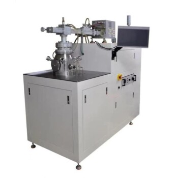
- RF PECVD System Radio Frequency Plasma Enhanced Chemical Vapor Deposition
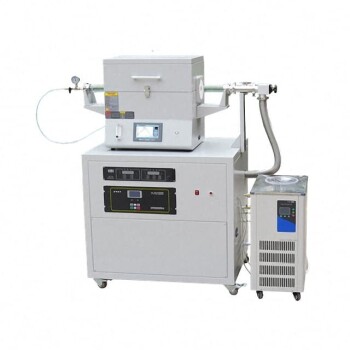
- Inclined Rotary Plasma Enhanced Chemical Deposition PECVD Tube Furnace Machine
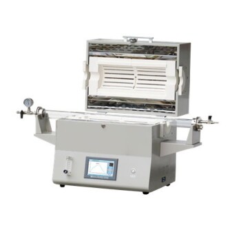
- Custom Made Versatile CVD Tube Furnace Chemical Vapor Deposition CVD Equipment Machine
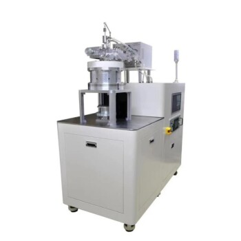
- HFCVD Machine System Equipment for Drawing Die Nano Diamond Coating
- Slide PECVD Tube Furnace with Liquid Gasifier PECVD Machine
People Also Ask
- What information does laboratory XRD provide for Gallium Sulfide? Master GaS Single Crystal Characterization
- What role does PECVD play in optical coatings? Essential for Low-Temp, High-Precision Film Deposition
- How is silicon dioxide (SiO2) used in PECVD applications? Key Roles in Microfabrication
- How does plasma enhanced CVD work? Achieve Low-Temperature, High-Quality Thin Film Deposition
- What is PECVD equipment? A Guide to Low-Temperature Thin-Film Deposition


