In essence, Chemical Vapor Deposition (CVD) is a high-performance manufacturing process used to deposit a thin, durable film of a solid material onto a surface, known as a substrate. This is achieved by introducing precursor gases into a high-temperature reaction chamber, where chemical reactions cause a new material layer to form on the substrate. Its most common applications are in the manufacturing of semiconductors, protective tool coatings, and advanced optical components.
The true value of CVD lies not just in adding a layer, but in creating a material with exceptional purity, uniformity, and specific properties that are often impossible to achieve with other methods. It is a foundational technology for building the high-performance components that power modern electronics and industry.

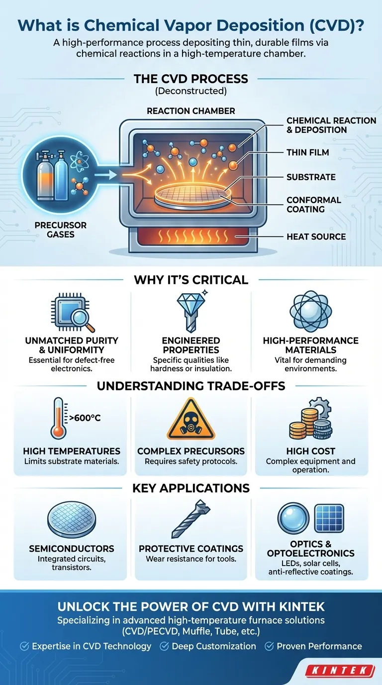
Deconstructing the CVD Process
To understand why CVD is so critical, you must first understand its fundamental mechanics. The process is a carefully controlled chemical synthesis that occurs on a microscopic level.
The Core Components
The CVD process relies on three key elements: a substrate, which is the object to be coated; precursor gases, which contain the atoms needed for the new film; and a controlled reaction chamber.
The substrate is placed inside the chamber, which is then sealed. The precursor gases are then introduced into this controlled environment.
The Chemical Reaction Phase
The chamber is heated to a specific, often very high, temperature. This thermal energy breaks down the precursor gases, causing their constituent atoms to become reactive.
These newly freed atoms then react with each other in the vapor phase, beginning to form the molecules of the desired coating material.
The Deposition Phase
As these new molecules are formed, they deposit onto all exposed surfaces of the cooler substrate, creating a solid, uniform thin film.
Because this process occurs via a gas that fills the entire chamber, the coating is highly conformal, meaning it can uniformly cover even complex, non-flat shapes. The thickness of the film is precisely controlled by managing the time, temperature, and gas flow.
Why CVD is a Critical Manufacturing Technology
CVD is not just another coating method; it is an enabling technology. It is chosen when the material properties of the final film are more important than anything else.
Achieving Unmatched Purity and Uniformity
Because the process starts with ultra-pure gases in a tightly controlled vacuum environment, the resulting films are exceptionally pure and free from defects. This is a non-negotiable requirement for applications like semiconductors, where a single impurity can ruin a microchip.
Engineering Superior Material Properties
CVD allows for the creation of materials with specific, engineered qualities. This includes depositing diamond-like carbon for extreme hardness on cutting tools, creating silicon dioxide layers for electrical insulation in circuits, or synthesizing materials for optoelectronics.
Creating High-Performance Materials
The process is used to produce some of the highest-performing materials available, including advanced ceramics, metals, and even synthetic diamond. These materials provide exceptional performance characteristics that are vital in demanding environments.
Understanding the Trade-offs
While powerful, CVD is not a universal solution. Its specialized nature comes with specific challenges and limitations that make it suitable for high-value applications.
High Temperature Requirements
Traditional CVD processes require very high temperatures, often exceeding 600°C (1112°F). This limits the types of substrate materials that can be used, as many materials cannot withstand such heat without being damaged or melting.
Precursor Gas Complexity
The precursor gases used in CVD can be highly toxic, flammable, or corrosive. This necessitates sophisticated safety protocols, specialized handling equipment, and robust exhaust management systems, adding to operational complexity.
Equipment and Process Cost
CVD reactors are complex, precision-engineered machines that are expensive to purchase and operate. The combination of high equipment cost, energy consumption, and safety requirements means CVD is typically reserved for components where performance justifies the investment.
Key Applications Across Industries
CVD's ability to create flawless, high-performance films has made it indispensable across several key technology sectors.
The Semiconductor Industry
This is the largest application of CVD. It is used at multiple stages to build the intricate layers of a modern integrated circuit, depositing the conductive, insulating, and semiconducting films that form transistors.
Protective and Hard Coatings
CVD is used to apply extremely hard and wear-resistant coatings to industrial cutting tools, drill bits, and engine components. These coatings dramatically increase the lifespan and performance of the parts, protecting them from friction, oxidation, and corrosion.
Optics and Optoelectronics
In optics, CVD is used to apply anti-reflective coatings on lenses. In optoelectronics, it is fundamental to manufacturing LEDs and the high-purity silicon films used in solar cells.
Making the Right Choice for Your Goal
Understanding when to leverage CVD depends entirely on your final objective.
- If your primary focus is cutting-edge electronics: CVD is essential for fabricating the ultra-pure, defect-free thin films required for microprocessors and memory chips.
- If your primary focus is mechanical durability: CVD is the premier choice for applying hard, wear-resistant coatings that protect critical components from failure.
- If your primary focus is advanced materials research: CVD provides a precise method for synthesizing novel materials and films with unique optical, electrical, or physical properties.
Ultimately, Chemical Vapor Deposition is the technology that builds materials from the atom up, enabling performance that defines modern innovation.
Summary Table:
| Aspect | Details |
|---|---|
| Definition | Process to deposit thin, durable films on substrates via chemical reactions in a high-temperature chamber. |
| Key Advantages | High purity, uniformity, conformal coating, and ability to engineer specific material properties. |
| Common Applications | Semiconductors, protective tool coatings, optical components, and advanced materials research. |
| Limitations | High temperature requirements, precursor gas complexity, and high equipment costs. |
Unlock the Power of CVD for Your Laboratory
At KINTEK, we specialize in delivering advanced high-temperature furnace solutions tailored to your unique needs. Leveraging our exceptional R&D and in-house manufacturing, we offer a comprehensive product line including CVD/PECVD Systems, Muffle, Tube, Rotary Furnaces, and Vacuum & Atmosphere Furnaces. Our strong deep customization capability ensures precise alignment with your experimental requirements, whether you're in semiconductors, protective coatings, or materials research.
Why Choose KINTEK?
- Expertise in CVD Technology: We provide reliable systems that enable superior thin film deposition with high purity and uniformity.
- Custom Solutions: From initial design to final implementation, we adapt our furnaces to meet your specific challenges.
- Proven Performance: Trusted by diverse laboratories for enhancing efficiency and achieving breakthrough results.
Ready to elevate your research and manufacturing processes? Contact us today to discuss how our CVD systems and other furnace solutions can drive your success!
Visual Guide
Related Products
- 915MHz MPCVD Diamond Machine Microwave Plasma Chemical Vapor Deposition System Reactor
- Custom Made Versatile CVD Tube Furnace Chemical Vapor Deposition CVD Equipment Machine
- MPCVD Machine System Reactor Bell-jar Resonator for Lab and Diamond Growth
- HFCVD Machine System Equipment for Drawing Die Nano Diamond Coating
- RF PECVD System Radio Frequency Plasma Enhanced Chemical Vapor Deposition
People Also Ask
- What factors influence the quality of diamond deposition in the MPCVD method? Master the Critical Parameters for High-Quality Diamond Growth
- What are some key features and benefits of the microwave plasma chemical vapor deposition system? Achieve Unmatched Material Synthesis
- What are the essential components of an MPCVD reactor for diamond film deposition? Unlock High-Quality Diamond Growth
- What is the basic principle of operation for the microwave plasma chemical vapor deposition system? Unlock High-Purity Material Growth
- What is the purpose of a microwave plasma chemical vapor deposition system? Grow High-Purity Diamonds and Advanced Materials


