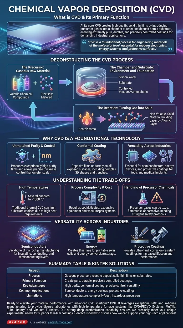
At its core, Chemical Vapor Deposition (CVD) is a sophisticated manufacturing process used to grow a high-quality, solid thin film on the surface of a material, known as a substrate. It achieves this by introducing precursor gases into a chamber, which then undergo a chemical reaction to deposit the desired material onto that substrate. Its primary function is to create extremely pure, durable, and precisely controlled coatings that enhance a material's properties for demanding industrial applications.
Chemical Vapor Deposition is not merely a coating technique; it is a foundational process for engineering materials at the molecular level. It enables the creation of the ultra-thin, high-performance layers that are essential for modern electronics, energy systems, and protective surfaces.
Deconstructing the CVD Process
To truly understand CVD, we must break it down into its fundamental components. The entire process occurs within a highly controlled environment to ensure the purity and quality of the final film.
The Precursor: The Gaseous Raw Material
The process begins with one or more precursor gases. These are volatile chemical compounds that contain the atoms of the material you wish to deposit.
These gases are precisely metered and introduced into a reaction chamber. The choice of precursor is critical, as it determines the composition of the final film and the conditions required for the reaction.
The Chamber and Substrate: The Environment and Foundation
The substrate is the object or material onto which the film will be grown. This could be a silicon wafer for a microchip, a medical implant, or a machine tool.
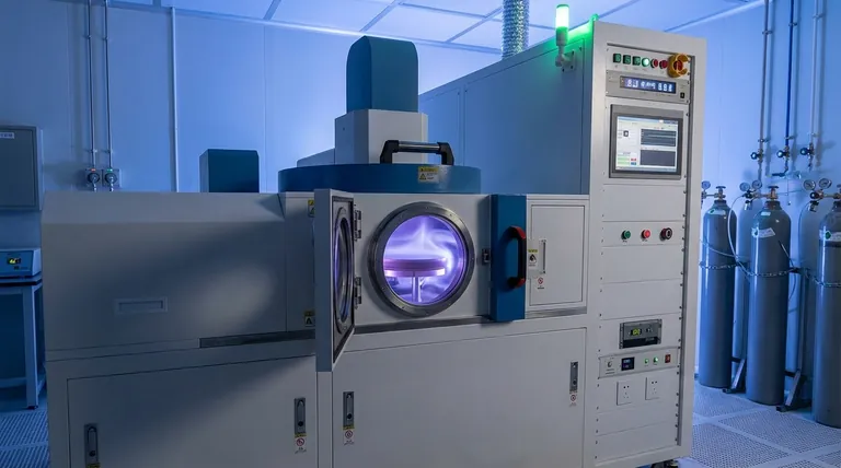
The substrate is placed inside a sealed reaction chamber, which is often a vacuum chamber. This controlled environment prevents contamination from unwanted atmospheric gases and allows for precise control over pressure and temperature.
The Reaction: Turning Gas into Solid
To initiate the deposition, energy is introduced into the chamber, typically in the form of high heat (thermal CVD) or plasma (plasma-assisted CVD).
This energy causes the precursor gases to decompose or react with each other on the heated surface of the substrate. This chemical reaction results in the formation of a non-volatile, solid material that bonds directly to the substrate, building up layer by atomic layer.
Why CVD is a Foundational Technology
CVD is not just one of many coating options; its unique capabilities make it indispensable in several high-tech fields. Its value lies in the quality and precision it delivers.
Unmatched Purity and Control
Because CVD is a chemical process built from a gaseous state, it can produce films of exceptionally high purity and structural quality, including single-crystal films.
The thickness of the deposited film can be controlled with extreme precision, often down to the nanometer scale, simply by managing the deposition time, gas flow, and temperature.
Conformal Coating: Covering Every Surface
A key advantage of CVD is its ability to produce conformal coatings. This means the film deposits uniformly across all exposed surfaces of the substrate, including complex, three-dimensional shapes and deep trenches.
This complete coverage is critical for protecting parts from corrosion and for ensuring the proper function of microscopic electronic components.
Versatility Across Industries
The applications for CVD are vast and growing:
- Semiconductors: It is the backbone of microchip manufacturing, used to deposit the insulating, conducting, and semiconducting layers on silicon wafers.
- Energy: It is used to create thin films for printable solar cells and other energy conversion and storage devices.
- Protective Coatings: It creates ultra-hard and corrosion-resistant coatings for cutting tools, engine parts, and medical implants to dramatically increase their lifespan and performance.
Understanding the Trade-offs
While powerful, CVD is not a universal solution. Acknowledging its limitations is key to using it effectively.
Requirement of High Temperatures
Traditional thermal CVD often requires very high temperatures (several hundred to over a thousand degrees Celsius) to drive the chemical reactions.
This can limit the types of substrate materials that can be used, as many polymers or lower-melting-point metals cannot withstand such heat without damage. Plasma-assisted variations can lower this temperature but add complexity.
Process Complexity and Cost
CVD systems are complex and expensive pieces of equipment. They require sophisticated vacuum, gas handling, and temperature control systems.
This high capital cost means CVD is typically reserved for applications where the performance benefits of the high-quality film justify the investment.
Handling of Precursor Chemicals
The precursor gases used in CVD can be toxic, flammable, or corrosive. The process requires stringent safety protocols for the storage, handling, and disposal of these chemicals and their byproducts.
Making the Right Choice for Your Goal
Selecting CVD depends entirely on whether its unique benefits align with your primary objective.
- If your primary focus is advanced electronics: CVD is non-negotiable for building the ultra-pure, precisely controlled thin layers required for modern semiconductors.
- If your primary focus is extreme material durability: CVD provides superior hard, wear-resistant, and corrosion-proof coatings for critical mechanical components.
- If your primary focus is next-generation optics or energy: CVD is a key enabling technology for producing the high-performance films needed for solar cells, LEDs, and specialized lenses.
Ultimately, understanding Chemical Vapor Deposition is understanding how we engineer and build the high-performance materials that define modern technology.
Summary Table:
| Aspect | Description |
|---|---|
| Process | Gaseous precursors react in a chamber to deposit solid thin films on substrates. |
| Primary Function | Create pure, durable, and precisely controlled coatings to enhance material properties. |
| Key Advantages | High purity, precise thickness control, conformal coating, versatility across industries. |
| Common Applications | Semiconductors, energy devices, protective coatings for tools and implants. |
| Limitations | High temperatures, process complexity, cost, and handling of hazardous precursors. |
Ready to elevate your material performance with advanced CVD solutions? KINTEK leverages exceptional R&D and in-house manufacturing to provide diverse laboratories with high-temperature furnace systems like CVD/PECVD Systems, Muffle, Tube, Rotary Furnaces, and Vacuum & Atmosphere Furnaces. Our strong deep customization capability ensures we precisely meet your unique experimental needs for superior thin-film coatings. Contact us today to discuss how we can support your high-tech applications!
Visual Guide
Related Products
- Custom Made Versatile CVD Tube Furnace Chemical Vapor Deposition CVD Equipment Machine
- MPCVD Machine System Reactor Bell-jar Resonator for Lab and Diamond Growth
- Multi Heating Zones CVD Tube Furnace Machine for Chemical Vapor Deposition Equipment
- 915MHz MPCVD Diamond Machine Microwave Plasma Chemical Vapor Deposition System Reactor
- Slide PECVD Tube Furnace with Liquid Gasifier PECVD Machine
People Also Ask
- What improvements can be made to the bonding force of gate dielectric films using a CVD tube furnace? Enhance Adhesion for Reliable Devices
- How does CVD tube furnace sintering enhance graphene growth? Achieve Superior Crystallinity and High Electron Mobility
- Which industries and research fields benefit from CVD tube furnace sintering systems for 2D materials? Unlock Next-Gen Tech Innovations
- What future trends are expected in the development of CVD tube furnaces? Discover Smarter, More Versatile Systems
- What are the key application fields of CVD tube furnaces? Unlock Precision in Thin-Film Synthesis


