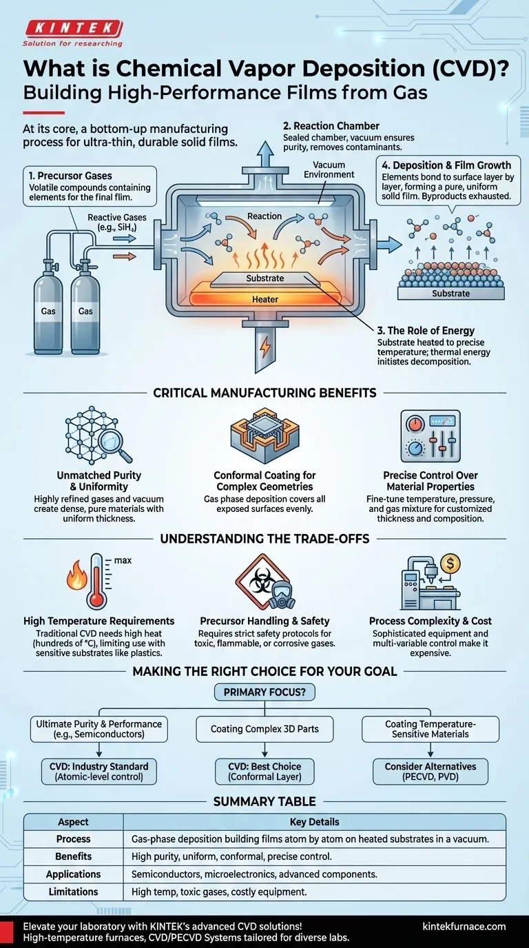
At its core, Chemical Vapor Deposition (CVD) is a manufacturing process used to grow ultra-thin, high-performance solid films on a surface. It works by introducing reactive gases, known as precursors, into a chamber where they undergo a chemical reaction and deposit a new material, layer by layer, onto a heated object or substrate. This method creates coatings that are exceptionally pure, durable, and uniform.
The crucial insight is that CVD is not simply "spraying" a coating on. It is a bottom-up fabrication process that literally builds a new solid material, atom by atom, directly onto a substrate from a gaseous state, offering unparalleled control over the final film's properties.
The Fundamental Principle: Building from Gas
CVD operates on a precise sequence of events inside a controlled environment. Understanding these steps reveals how it achieves such high-quality results.
The Precursor Gases
The process begins with precursor gases. These are volatile chemical compounds that contain the specific elements needed for the final film.
For example, to create a silicon film, a precursor like silane gas (SiH₄) might be used. These gases are the raw building blocks of the coating.
The Reaction Chamber
The precursors are injected into a sealed reaction chamber, which is typically held under a vacuum (well below atmospheric pressure).
Inside the chamber is the object to be coated, known as the substrate. The vacuum environment is critical for ensuring purity by removing any unwanted particles or gases that could contaminate the film.
The Role of Energy
The substrate is heated to a precise, elevated temperature. This thermal energy is the catalyst that drives the entire process.
When the precursor gases come into contact with the hot substrate, the energy causes them to decompose or react with each other. The chemical bonds within the precursor molecules break apart.
Deposition and Film Growth
Once the precursor gases break down, the desired solid elements bond directly to the substrate's surface. The other elements from the precursor gas form volatile byproducts that are exhausted from the chamber.
This process, called deposition, builds the film one atomic or molecular layer at a time. Over time, these layers accumulate to form a completely new, solid film that is perfectly bonded to the substrate.
Why CVD is a Critical Manufacturing Process
CVD is not just one of many coating methods; its unique characteristics make it indispensable in high-technology fields, particularly for semiconductors.
Unmatched Purity and Uniformity
Because the film is "grown" in a vacuum from highly refined gases, the resulting material is exceptionally pure and dense.
The process also ensures the film has a highly uniform thickness across the entire substrate, which is essential for the reliable performance of microelectronics.
Conformal Coating for Complex Geometries
Since the deposition happens from a gas phase, CVD can coat all exposed surfaces of a substrate evenly.
This ability to create a conformal coating is vital for covering intricate, three-dimensional structures found on microchips and other complex components.
Precise Control Over Material Properties
By carefully managing the process variables—such as temperature, pressure, and the mixture of precursor gases—engineers can precisely control the film's final properties.
This includes its thickness, chemical composition, and microstructure, allowing for the creation of highly customized materials for specific applications.
Understanding the Trade-offs
While powerful, CVD is not a universal solution. Its requirements introduce specific limitations and challenges.
High Temperature Requirements
Traditional thermal CVD often requires very high temperatures (several hundred to over a thousand degrees Celsius) to initiate the chemical reaction.
These temperatures can damage sensitive substrates, such as plastics or certain electronic components, limiting the materials that can be coated. This has led to the development of lower-temperature variants like Plasma-Enhanced CVD (PECVD).
Precursor Handling and Safety
The precursor gases used in CVD can be highly toxic, flammable, or corrosive.
This necessitates sophisticated safety protocols, specialized handling equipment, and complex exhaust management systems, which add to the cost and complexity of the operation.
Process Complexity and Cost
Achieving a flawless, uniform film requires precise and stable control over multiple variables simultaneously. The equipment is sophisticated and expensive.
This makes CVD a less cost-effective choice for applications where the ultimate purity and performance are not the primary requirements.
Making the Right Choice for Your Goal
Selecting a deposition method depends entirely on the technical and economic goals of your project.
- If your primary focus is ultimate purity and performance (e.g., semiconductors): CVD is the industry standard because its atomic-level control delivers the necessary quality.
- If your primary focus is coating complex, three-dimensional parts: CVD's gas-phase nature provides a uniform, conformal layer that line-of-sight methods cannot match.
- If your primary focus is coating temperature-sensitive materials: You must consider lower-temperature CVD variants or explore entirely different methods, such as Physical Vapor Deposition (PVD).
Ultimately, chemical vapor deposition is a foundational technology that empowers engineers to construct the high-performance materials that define modern electronics and advanced components.
Summary Table:
| Aspect | Key Details |
|---|---|
| Process | Gas-phase deposition building films atom by atom on heated substrates in a vacuum chamber. |
| Benefits | High purity, uniform thickness, conformal coating for complex shapes, precise material control. |
| Applications | Semiconductors, microelectronics, advanced components requiring durable, high-performance films. |
| Limitations | High temperatures may damage sensitive substrates; requires toxic gas handling and costly equipment. |
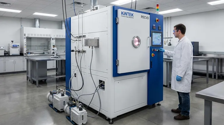
Elevate your laboratory's capabilities with KINTEK's advanced CVD solutions! Leveraging exceptional R&D and in-house manufacturing, we provide high-temperature furnaces, including CVD/PECVD Systems, tailored for diverse labs. Our strong deep customization ensures precise alignment with your unique experimental needs, delivering superior film quality and efficiency. Ready to optimize your deposition processes? Contact us today to discuss how our expertise can benefit your projects!
Visual Guide
Related Products
- Custom Made Versatile CVD Tube Furnace Chemical Vapor Deposition CVD Equipment Machine
- Multi Heating Zones CVD Tube Furnace Machine for Chemical Vapor Deposition Equipment
- Slide PECVD Tube Furnace with Liquid Gasifier PECVD Machine
- RF PECVD System Radio Frequency Plasma Enhanced Chemical Vapor Deposition
- MPCVD Machine System Reactor Bell-jar Resonator for Lab and Diamond Growth
People Also Ask
- Why are CVD tube furnace sintering systems indispensable for 2D material research and production? Unlock Atomic-Scale Precision
- What customization options are available for CVD tube furnaces? Tailor Your System for Superior Material Synthesis
- What is a CVD tube furnace and what is its primary function? Discover Precision Thin-Film Deposition
- What are the key features of CVD tube furnaces for 2D material processing? Unlock Precision Synthesis for Superior Materials
- How does CVD tube furnace sintering enhance graphene growth? Achieve Superior Crystallinity and High Electron Mobility


