In essence, Chemical Vapor Deposition (CVD) is a process defined by its versatility, capable of depositing materials in several distinct structural forms. The primary structural varieties are amorphous, which lacks long-range atomic order, and polycrystalline, which consists of many small, interconnected crystal grains. CVD can also produce more complex, highly-ordered structures like single-crystal films and specialized nanoscale morphologies such as nanotubes and quantum dots.
The true power of CVD is not just in depositing a specific material, but in precisely controlling its atomic structure. This structural control—from disordered amorphous films to perfect single crystals—is what ultimately dictates the material's properties and determines its viability for a given application.

The Fundamental Structural Categories
Understanding the structural outcome of a CVD process is critical because structure dictates function. A silicon film, for example, will have vastly different electronic properties depending on whether it is amorphous, polycrystalline, or a single crystal.
Amorphous Films
An amorphous material lacks a defined, repeating crystalline structure. The atoms are arranged in a disordered, random fashion, similar to the structure of glass.
This lack of long-range order makes amorphous films ideal for applications where perfect crystal structure is not required or is even undesirable. They are often used for optical coatings and are crucial for flexible electronics, where a rigid crystal lattice would fail.
Polycrystalline Films
A polycrystalline film is composed of numerous small crystal grains, each with an ordered internal structure. However, these individual grains are randomly oriented with respect to one another.
This structure represents a middle ground, offering better electronic and mechanical properties than amorphous materials without the high cost and complexity of producing a perfect single crystal. It is the workhorse structure for applications like solar panels and many types of electronic device components. Synthetic diamond films, for instance, are often polycrystalline.
Epitaxial (Single-Crystal) Films
Though not explicitly a "variety" in the same way, CVD is a primary method for achieving epitaxial growth, which produces a single-crystal film. In this process, the deposited film continues the crystal lattice of the underlying substrate without interruption.
This creates a perfect, defect-free crystal structure that is essential for high-performance applications. Modern microelectronics, such as the silicon transistors in a CPU, rely entirely on the superior electronic properties of single-crystal films.
Advanced and Nanoscale Structures
Beyond traditional films, CVD is instrumental in fabricating materials with unique, engineered morphologies at the nanoscale.
Nanowires and Nanotubes
CVD can be controlled to promote one-dimensional growth, resulting in structures like nanowires and carbon nanotubes. These materials have exceptionally high aspect ratios and unique properties.
Their applications are found at the frontier of technology, including next-generation electronics, high-strength composites, and advanced sensor technologies.
Quantum Dots (Nanocrystals)
The process can also be used to create quantum dots, which are semiconductor nanocrystals so small that their electronic and optical properties are governed by quantum mechanics.
These zero-dimensional structures are enabling breakthroughs in medical imaging, high-efficiency solar cells, and vibrant display technologies like QLED TVs.
Understanding the Trade-offs: Structure vs. Application
Choosing a material structure is always a matter of balancing performance requirements against manufacturing complexity and cost. Each structural type comes with inherent trade-offs.
Amorphous: Flexibility and Uniformity
The key advantage of amorphous films is their ability to be deposited uniformly over large, non-crystalline, and even flexible substrates. However, their disordered structure leads to inferior electronic properties compared to their crystalline counterparts.
Polycrystalline: The Versatile Workhorse
Polycrystalline films offer a practical compromise. They provide significantly better performance than amorphous materials and are far easier and cheaper to produce than single crystals. The primary limitation is that the boundaries between crystal grains can impede electron flow or act as failure points.
Single-Crystal: The Peak of Performance
For maximum performance, nothing surpasses a single-crystal structure. The absence of grain boundaries allows for unparalleled electronic and optical properties. This performance comes at a high cost, requiring a compatible single-crystal substrate and precise process control.
Choosing the Right Structure for Your Application
Your technical goal will directly determine the most appropriate material structure to pursue.
- If your primary focus is high-performance electronics: Single-crystal (epitaxial) growth is non-negotiable for achieving the necessary device speed and efficiency.
- If your primary focus is cost-effective, large-area devices like solar panels: Polycrystalline films offer the best balance of electronic performance and manufacturability.
- If your primary focus is flexible devices or simple optical coatings: Amorphous films provide the required mechanical properties and uniformity over non-crystalline substrates.
- If your primary focus is novel quantum or nanoscale devices: You will need to employ specialized CVD techniques to create structures like quantum dots or carbon nanotubes.
Ultimately, mastering CVD is about intentionally selecting the material structure that directly enables your desired technological outcome.
Summary Table:
| Structural Variety | Key Characteristics | Common Applications |
|---|---|---|
| Amorphous Films | Disordered atomic structure, uniform deposition | Optical coatings, flexible electronics |
| Polycrystalline Films | Multiple crystal grains, cost-effective | Solar panels, electronic devices |
| Single-Crystal Films | Perfect crystal lattice, high performance | Microelectronics, CPUs |
| Nanoscale Structures (e.g., nanotubes, quantum dots) | Unique quantum properties, high aspect ratios | Sensors, composites, displays |
Ready to elevate your lab's capabilities with tailored CVD solutions? At KINTEK, we leverage exceptional R&D and in-house manufacturing to provide advanced high-temperature furnace solutions like Muffle, Tube, Rotary Furnaces, Vacuum & Atmosphere Furnaces, and CVD/PECVD Systems. Our deep customization capabilities ensure we meet your unique experimental needs, helping you achieve precise structural control for superior material properties. Contact us today to discuss how we can support your projects and drive innovation in your field!
Visual Guide

Related Products
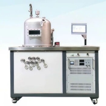
- RF PECVD System Radio Frequency Plasma Enhanced Chemical Vapor Deposition
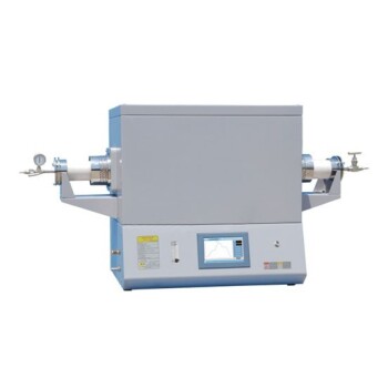
- Custom Made Versatile CVD Tube Furnace Chemical Vapor Deposition CVD Equipment Machine
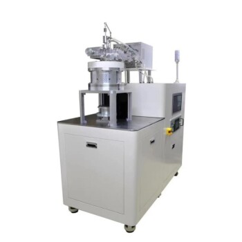
- Inclined Rotary Plasma Enhanced Chemical Deposition PECVD Tube Furnace Machine
- Multi Heating Zones CVD Tube Furnace Machine for Chemical Vapor Deposition Equipment
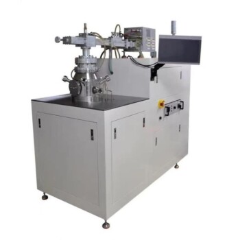
- Slide PECVD Tube Furnace with Liquid Gasifier PECVD Machine
People Also Ask
- What is PECVD and how does it differ from traditional CVD? Unlock Low-Temperature Thin Film Deposition
- How does plasma vapor deposition work? A Low-Temperature Solution for Advanced Coatings
- What is the second benefit of deposition within a discharge in PECVD? Enhance Film Quality with Ion Bombardment
- What information does laboratory XRD provide for Gallium Sulfide? Master GaS Single Crystal Characterization
- What gases are used in the PECVD system? Optimize Thin Film Deposition with Precise Gas Selection

