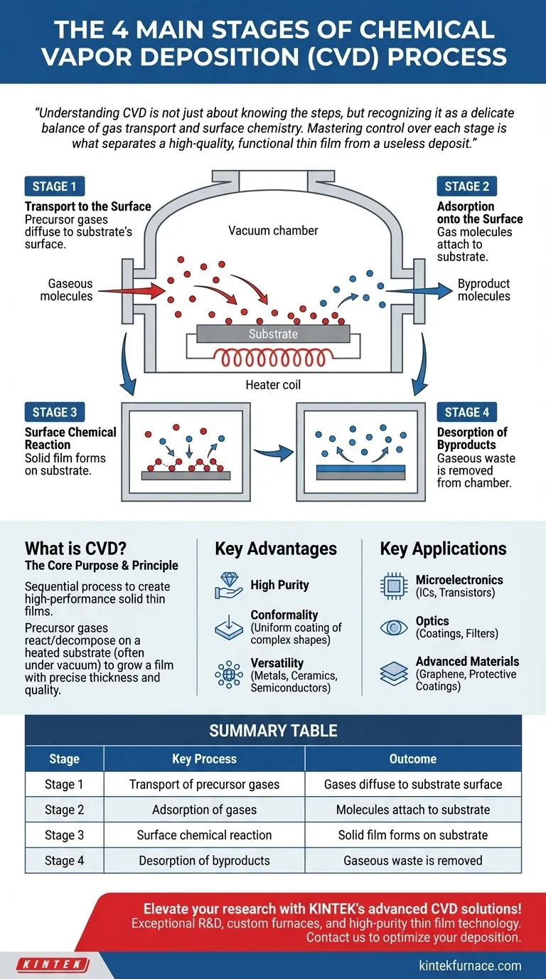
At its core, Chemical Vapor Deposition (CVD) is a sequential, four-stage process. First, reactant gases diffuse through the chamber to the substrate's surface. Second, these gases are adsorbed onto that surface. Third, a chemical reaction occurs, forming the solid film. Finally, the gaseous byproducts of that reaction are desorbed and removed from the chamber.
Understanding CVD is not just about knowing the steps, but recognizing it as a delicate balance of gas transport and surface chemistry. Mastering control over each stage is what separates a high-quality, functional thin film from a useless deposit.
What is Chemical Vapor Deposition?
Chemical Vapor Deposition is a highly versatile manufacturing process used to create high-performance, solid thin films on a substrate. It is the backbone of many advanced industries.
The Core Purpose
The primary function of CVD is to grow a layer of material on a base object, or substrate. This layer can provide protective qualities, like resistance to corrosion, or grant specific electronic or optical properties.
The Fundamental Principle
The process involves introducing precursor gases into a reaction chamber, which is typically under vacuum and held at a high temperature. These gases react or decompose upon contact with the heated substrate, forming a solid film that bonds to the surface. The film's thickness and quality are precisely controlled by factors like temperature, pressure, gas concentration, and deposition time.
Deconstructing the Four Stages of Deposition
The entire CVD process can be broken down into four distinct, sequential events. The efficiency of each stage directly impacts the quality of the final film.
Stage 1: Transport to the Surface
First, the reactant gases, also known as precursors, must travel from the gas inlet of the chamber to the immediate vicinity of the substrate. This mass transport happens through diffusion and convection, governed by the fluid dynamics inside the chamber.
Stage 2: Adsorption onto the Surface
Once the precursor gas molecules are near the substrate, they must physically attach to its surface. This process is called adsorption. Without this crucial step, the molecules would simply bounce off, and no chemical reaction could take place.
Stage 3: Surface Chemical Reaction
This is the film-forming stage. Energized by the substrate's high temperature, the adsorbed precursor molecules undergo chemical reactions. They may decompose or react with other adsorbed molecules to form the desired solid material, which then nucleates and grows into a continuous film.
Stage 4: Desorption of Byproducts
Most chemical reactions produce waste products. In CVD, these are typically other gases. These gaseous byproducts must detach from the surface (a process called desorption) and be transported away. If byproducts are not removed efficiently, they can contaminate the film or hinder the deposition of new material.
Understanding the Trade-offs
While powerful, CVD is not a universal solution. Its advantages are balanced by specific operational requirements and limitations.
Key Advantages of CVD
The process is valued for its ability to produce high-purity films with excellent structural quality.
Perhaps its most significant benefit is conformality. Because the precursor is a gas, it can coat complex, three-dimensional shapes uniformly, a feat that is difficult for line-of-sight deposition methods.
CVD is also highly versatile, capable of depositing a vast range of materials, including metals, ceramics, and semiconductors, on nearly any substrate that can withstand the heat.
Inherent Limitations and Considerations
The most significant constraint of traditional CVD is its reliance on high temperatures. This can damage or warp temperature-sensitive substrates, such as plastics or certain pre-processed semiconductor wafers.
The process also requires the use of precursor gases that can be volatile, toxic, or corrosive. This necessitates complex and expensive equipment for safe handling, delivery, and exhaust management.
Finally, most CVD processes operate under a vacuum, adding to the cost and complexity of the equipment and increasing processing time.
Key Applications of CVD
The unique capabilities of CVD have made it indispensable across several high-tech fields.
Microelectronics
CVD is fundamental to the semiconductor industry. It is used to deposit the insulating (dielectric), conducting, and semiconducting layers that form integrated circuits, transistors, and other microelectronic components.
Optics
The process is used to create high-performance optical coatings. This includes anti-reflective coatings on lenses, highly reflective films for mirrors, and specialized optical filters.
Advanced Materials and Coatings
CVD is used to create some of the most advanced materials available. This includes growing synthetic diamond and graphene films for cutting tools and sensors, as well as depositing hard, protective coatings on industrial parts to shield them from oxidation and wear.
How to Apply This to Your Project
Understanding these stages allows you to better diagnose issues and select the right process for your goal.
- If your primary focus is creating ultra-pure, dense films for semiconductors: The chemical reaction pathway of CVD ensures superior material quality and atomic-level control compared to most physical methods.
- If your primary focus is coating complex, three-dimensional parts uniformly: CVD's non-line-of-sight deposition is a critical advantage, ensuring complete and even coverage on all exposed surfaces.
- If your primary focus is coating heat-sensitive materials: You must investigate low-temperature variants like Plasma-Enhanced CVD (PECVD) or consider alternative deposition technologies entirely.
By viewing CVD as a sequence of controlled physical and chemical events, you can better optimize the process to achieve your desired material properties.
Summary Table:
| Stage | Key Process | Outcome |
|---|---|---|
| 1 | Transport of precursor gases | Gases diffuse to substrate surface |
| 2 | Adsorption of gases | Molecules attach to substrate |
| 3 | Surface chemical reaction | Solid film forms on substrate |
| 4 | Desorption of byproducts | Gaseous waste is removed |
Elevate your research with KINTEK's advanced CVD solutions! Leveraging exceptional R&D and in-house manufacturing, we provide diverse laboratories with high-temperature furnace systems like our CVD/PECVD Systems, Muffle, Tube, Rotary, Vacuum & Atmosphere Furnaces. Our strong deep customization capability ensures precise alignment with your unique experimental needs, delivering high-purity, conformal thin films for applications in microelectronics, optics, and advanced materials. Contact us today to discuss how we can optimize your deposition processes and achieve superior results!
Visual Guide
Related Products
- 915MHz MPCVD Diamond Machine Microwave Plasma Chemical Vapor Deposition System Reactor
- Custom Made Versatile CVD Tube Furnace Chemical Vapor Deposition CVD Equipment Machine
- RF PECVD System Radio Frequency Plasma Enhanced Chemical Vapor Deposition
- MPCVD Machine System Reactor Bell-jar Resonator for Lab and Diamond Growth
- HFCVD Machine System Equipment for Drawing Die Nano Diamond Coating
People Also Ask
- What factors influence the quality of diamond deposition in the MPCVD method? Master the Critical Parameters for High-Quality Diamond Growth
- What is the basic principle of operation for the microwave plasma chemical vapor deposition system? Unlock High-Purity Material Growth
- What are the main components of an MPCVD machine? Unlock the Secrets of Diamond Synthesis
- What are the essential components of an MPCVD reactor system? Build a Pristine Environment for High-Purity Materials
- What is the MPCVD method and why is it considered effective for diamond deposition? Superior Purity & High Growth Rates


