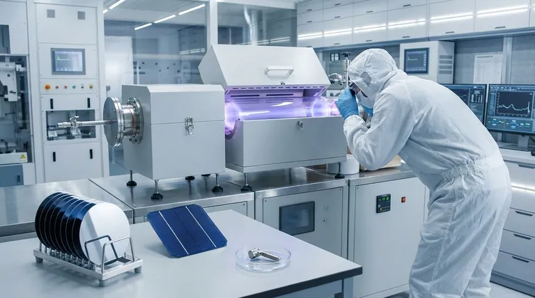
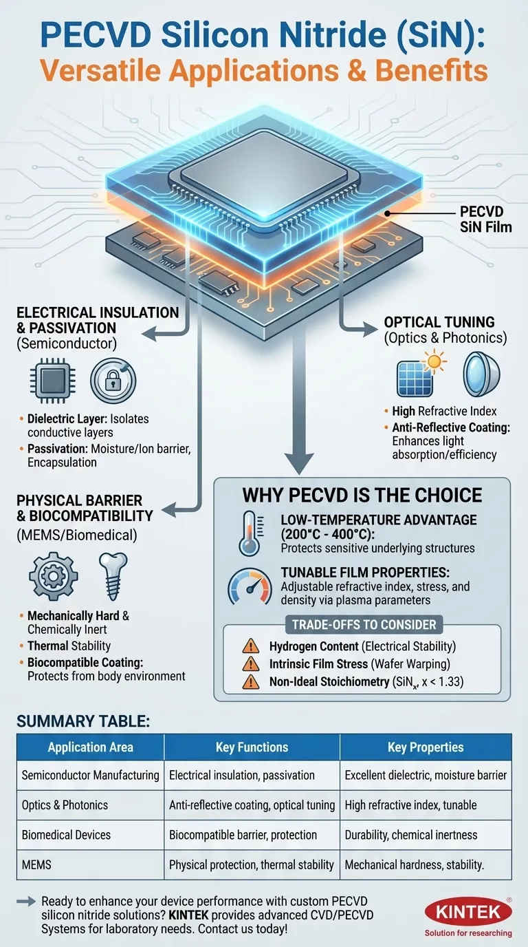
At its core, silicon nitride (SiN) deposited via Plasma-Enhanced Chemical Vapor Deposition (PECVD) is a versatile thin film used primarily for device protection and performance tuning. Its most common applications are in semiconductor manufacturing as an insulating and passivation layer, in optics as an anti-reflective coating, and in biomedical devices as a durable, biocompatible barrier. The key advantage of the PECVD method is its low-temperature nature, which allows this robust material to be deposited on sensitive, pre-existing device structures without damaging them.
The true value of PECVD silicon nitride lies not in any single property, but in its unique combination of being an excellent electrical insulator, a tough physical barrier, and an optically useful material—all achievable at temperatures low enough to be compatible with modern electronics fabrication.
The Core Functions of PECVD Silicon Nitride
To understand its wide range of applications, it's best to think of PECVD SiN in terms of its three primary functions: electrical insulation, physical protection, and optical modification.
As a Dielectric and Passivation Layer
In semiconductor manufacturing, PECVD SiN serves as a superior electrical insulator, or dielectric. It is used to isolate conductive layers within an integrated circuit, preventing electrical "shorting" between metal lines.
Its most critical role, however, is passivation. A final layer of SiN acts as a hermetic seal, providing a robust barrier that encapsulates the sensitive microchip. This protects the device from moisture, mobile ions like sodium, and other corrosive elements that would otherwise cause device failure.
As a Robust Physical Barrier
PECVD SiN is mechanically hard and chemically inert, making it an exceptional protective coating. This property is leveraged in Micro-Electro-Mechanical Systems (MEMS), where the film's thermal stability and strength are essential for high-temperature applications.
This same durability and chemical inertness make it highly biocompatible. It is used to coat medical implants and devices, protecting them from the corrosive environment of the human body and protecting the body from the device itself.
As an Optical Tuning Layer
Silicon nitride has a high refractive index, a property that is heavily exploited in optics and photonics.
Its most widespread optical application is as an anti-reflective coating, particularly in the manufacturing of solar cells. By depositing a thin, precisely controlled layer of SiN on the surface of a solar cell, manufacturers can minimize light reflection and maximize the amount of light absorbed, thereby increasing the cell's efficiency.
Why PECVD is the Deposition Method of Choice
The choice of PECVD is just as important as the choice of silicon nitride. The process itself unlocks the material's full potential for modern applications.
The Low-Temperature Advantage
Traditional methods for depositing high-quality silicon nitride require temperatures in excess of 700°C. Such heat would destroy the delicate transistors and metal wiring already built on a silicon wafer.
PECVD operates at much lower temperatures, typically between 200°C and 400°C. This allows a dense, high-quality SiN film to be deposited late in the manufacturing process without damaging the underlying integrated circuit.
Tunable Film Properties
The PECVD process offers a high degree of control. By adjusting the plasma parameters—such as gas composition, pressure, and power—engineers can precisely tune the properties of the resulting SiN film.
This allows them to adjust the film's refractive index for optical coatings, its internal stress to prevent wafer warping, and its density for barrier performance, tailoring the film for its specific application.
Understanding the Trade-offs
While incredibly useful, PECVD SiN is not a perfect material. A true expert understands its limitations.
Inherent Hydrogen Content
Because PECVD uses hydrogen-containing precursor gases (like silane and ammonia), the resulting films contain a significant amount of hydrogen. This incorporated hydrogen can impact the long-term electrical stability of sensitive transistors. For the most critical gate dielectric layers, purer, high-temperature nitrides are often preferred.
Intrinsic Film Stress
PECVD SiN films inherently have internal stress, which can be either compressive or tensile. If not properly managed by tuning the deposition process, high stress can cause the silicon wafer to bend or even lead to film delamination and cracking, compromising the device.
Non-Ideal Stoichiometry
The chemical formula for pure, stoichiometric silicon nitride is Si₃N₄. PECVD films are often "silicon-rich," meaning they have a formula of SiNₓ where 'x' is less than 1.33. This deviation affects the film's electrical properties, optical constants, and chemical etch rates, a factor that must be accounted for in device design and fabrication.
Making the Right Choice for Your Goal
Your application determines which property of PECVD SiN is most important.
- If your primary focus is electrical isolation and device protection: Leverage its excellent dielectric strength and low permeability to use it as a final passivation layer for integrated circuits, LEDs, or other sensitive electronics.
- If your primary focus is modifying optical properties: Utilize its high, tunable refractive index to design and deposit anti-reflective coatings for solar cells, sensors, or other optical components.
- If your primary focus is creating a durable, biocompatible coating: Rely on its high hardness, chemical inertness, and proven biocompatibility to protect MEMS devices or medical implants from harsh environments.
Ultimately, PECVD silicon nitride provides a powerful and adaptable solution for protecting and enhancing high-performance devices.
Summary Table:
| Application Area | Key Functions | Key Properties |
|---|---|---|
| Semiconductor Manufacturing | Electrical insulation, passivation | Excellent dielectric, moisture barrier |
| Optics and Photonics | Anti-reflective coating, optical tuning | High refractive index, tunable |
| Biomedical Devices | Biocompatible barrier, protection | Durability, chemical inertness |
| MEMS | Physical protection, thermal stability | Mechanical hardness, stability |
Ready to enhance your device performance with custom PECVD silicon nitride solutions? KINTEK leverages exceptional R&D and in-house manufacturing to provide advanced high-temperature furnace systems, including CVD/PECVD Systems, tailored for diverse laboratory needs. Our strong deep customization capability ensures precise solutions for your unique experimental requirements in semiconductors, optics, and biomedical applications. Contact us today to discuss how we can help optimize your processes and achieve superior results!
Visual Guide
Related Products
- Slide PECVD Tube Furnace with Liquid Gasifier PECVD Machine
- Inclined Rotary Plasma Enhanced Chemical Deposition PECVD Tube Furnace Machine
- RF PECVD System Radio Frequency Plasma Enhanced Chemical Vapor Deposition
- Inclined Rotary Plasma Enhanced Chemical Deposition PECVD Tube Furnace Machine
People Also Ask
- What plasma source is used in PE-CVD tube furnaces? Unlock Low-Temperature, High-Quality Deposition
- How does a hydrogen reduction environment in an industrial tube furnace facilitate gold-copper alloy microspheres?
- What is plasma in the context of PECVD? Unlock Low-Temperature Thin Film Deposition
- What are the advantages of using a tube furnace CVD system for Cu(111)/graphene? Superior Scalability and Quality
- How does PECVD equipment contribute to TOPCon bottom cells? Mastering Hydrogenation for Maximum Solar Efficiency


