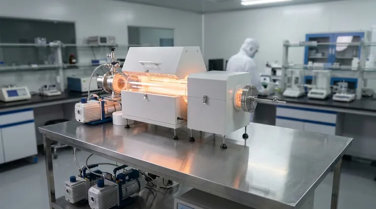
In nanofabrication, Plasma-Enhanced Chemical Vapor Deposition (PECVD) is a cornerstone technology used to deposit thin films of critical materials like silicon dioxide, silicon nitride, and amorphous silicon. Its primary applications are creating insulating layers for transistors, such as in shallow trench and sidewall isolation, as well as fabricating optical coatings, solar cells, and protective layers. The defining advantage of PECVD is its ability to perform these depositions at low temperatures, protecting delicate, pre-existing structures on a microchip.
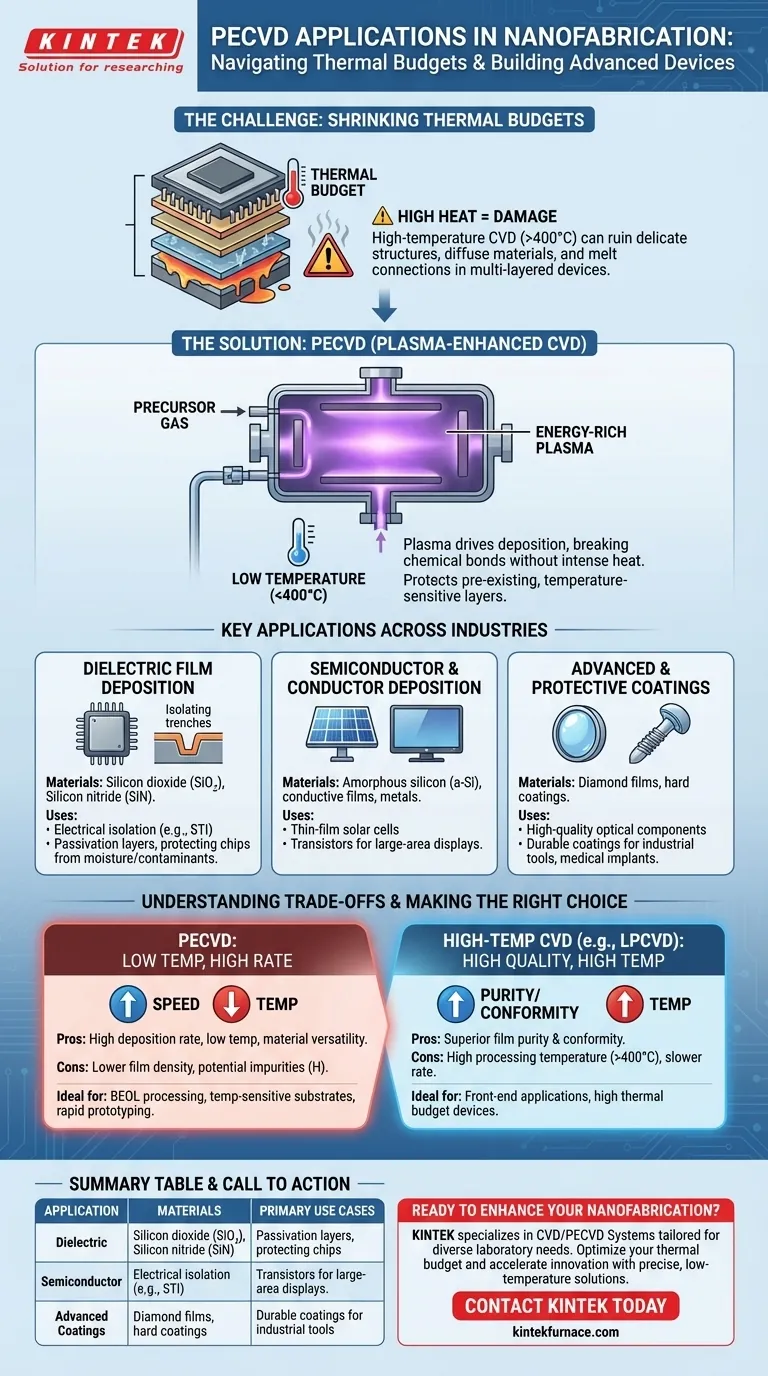
As nanoscale devices become more complex, the total amount of heat a device can tolerate—its "thermal budget"—shrinks dramatically. PECVD's fundamental value lies in using an energy-rich plasma, rather than intense heat, to drive film deposition, making it an indispensable tool for modern, multi-layered device fabrication.
The Core Problem PECVD Solves: The Thermal Budget Constraint
In nanofabrication, devices are built vertically, layer by layer. Each new processing step must not damage or alter the layers already in place. This is where temperature becomes a critical limiting factor.
Why High Temperatures Are a Problem
High-temperature processes, common in traditional chemical vapor deposition (CVD), can cause previously deposited materials to diffuse into one another, ruining carefully engineered junctions. They can also damage or melt low-melting-point metals used for electrical connections, rendering the device useless.
How PECVD Bypasses Heat
PECVD circumvents this issue by introducing energy in a different form: plasma. An electrical field is used to ionize precursor gases, creating a highly reactive plasma. This plasma provides the necessary energy to break chemical bonds and drive the deposition reaction on the substrate surface, all without requiring high substrate temperatures.
This low-temperature capability (typically below 400°C) is not just an advantage; it is often a requirement for manufacturing advanced semiconductor devices.
Key Applications Across Industries
PECVD's combination of low-temperature processing and material versatility makes it a workhorse technology for depositing a wide range of essential films.
Dielectric Film Deposition
This is the most common application in microelectronics. PECVD is used to deposit insulating materials like silicon dioxide (SiO₂) and silicon nitride (SiN). These films are used for electrical isolation between components, such as in shallow trench isolation (STI), and as protective passivation layers that shield the final chip from moisture and contaminants.
Semiconductor and Conductor Deposition
The process is also used to deposit semiconductor films like amorphous silicon (a-Si), which is a key material in thin-film solar cells and the transistors used in large-area displays. In some cases, PECVD can also be adapted to deposit conductive films and metals.
Advanced and Protective Coatings
Beyond microchips, PECVD's versatility allows it to produce highly durable and specialized films. This includes creating high-quality diamond films for advanced optical and electronic components or depositing hard, protective coatings for industrial tools and medical implants.
Understanding the Trade-offs
While powerful, PECVD is not the optimal solution for every scenario. The choice of a deposition method involves balancing competing factors of temperature, quality, and speed.
Quality and Deposition Rate
Compared to high-temperature methods like Low-Pressure CVD (LPCVD), PECVD films are generally deposited at a much higher rate. However, this speed can come at the cost of film quality. PECVD films are often less dense and may contain impurities like hydrogen from the precursor gases, which can affect electrical performance in some sensitive applications.
Temperature as the Deciding Factor
The choice between PECVD and a higher-temperature method almost always comes down to the thermal budget. If a device structure contains materials that cannot withstand heat above 400°C, PECVD becomes the default and necessary choice. The trade-off in film density is accepted to avoid catastrophic failure of the device.
Unmatched Material Versatility
A key strength of PECVD is its ability to deposit a vast library of materials, including oxides, nitrides, semiconductors, and even polymers. This flexibility makes it invaluable for research and development, where engineers need to experiment with novel material combinations and device architectures.
Making the Right Choice for Your Goal
Selecting the correct deposition technique is critical for successful fabrication. Your decision should be guided by the specific constraints and objectives of your process.
- If your primary focus is backend-of-line (BEOL) processing or temperature-sensitive substrates: PECVD is your essential tool due to its low-temperature operation, which protects metallic interconnects and other fragile structures.
- If your primary focus is the highest possible film purity and conformity for front-end applications: LPCVD may be superior, provided your device's thermal budget can withstand the high processing temperatures.
- If your primary focus is rapid prototyping or material exploration: PECVD's versatility and high deposition rates make it an ideal choice for developing and testing new processes and devices quickly.
Ultimately, mastering PECVD is about leveraging its low-temperature advantage to build complex, multi-layered nanostructures that would otherwise be impossible to fabricate.
Summary Table:
| Application Area | Key Materials Deposited | Primary Use Cases |
|---|---|---|
| Dielectric Film Deposition | Silicon dioxide (SiO₂), Silicon nitride (SiN) | Electrical isolation, Passivation layers |
| Semiconductor and Conductor Deposition | Amorphous silicon (a-Si) | Thin-film solar cells, Transistors for displays |
| Advanced and Protective Coatings | Diamond films, Hard coatings | Optical components, Industrial tools, Medical implants |
Ready to enhance your nanofabrication with precise, low-temperature solutions? KINTEK specializes in advanced high-temperature furnace systems, including CVD/PECVD Systems, tailored for diverse laboratory needs. Leveraging our exceptional R&D and in-house manufacturing, we offer deep customization to meet your unique experimental requirements. Contact us today to discuss how our PECVD expertise can optimize your thermal budget and accelerate your innovations in microelectronics, solar energy, and beyond!
Visual Guide
Related Products
- RF PECVD System Radio Frequency Plasma Enhanced Chemical Vapor Deposition
- Slide PECVD Tube Furnace with Liquid Gasifier PECVD Machine
- Inclined Rotary Plasma Enhanced Chemical Deposition PECVD Tube Furnace Machine
- Inclined Rotary Plasma Enhanced Chemical Deposition PECVD Tube Furnace Machine
- Cylindrical Resonator MPCVD Machine System for Lab Diamond Growth
People Also Ask
- What are the advantages of PECVD in film deposition? Achieve Low-Temp, High-Quality Coatings
- What are the applications of plasma enhanced chemical vapor deposition? Key Uses in Electronics, Optics & Materials
- What is PECVD specification? A Guide to Choosing the Right System for Your Lab
- What is the role of RF power in PECVD and how does the RF-PECVD process work? Master Thin Film Deposition Control
- What are some promising applications of PECVD-prepared 2D materials? Unlock Advanced Sensing and Optoelectronics


