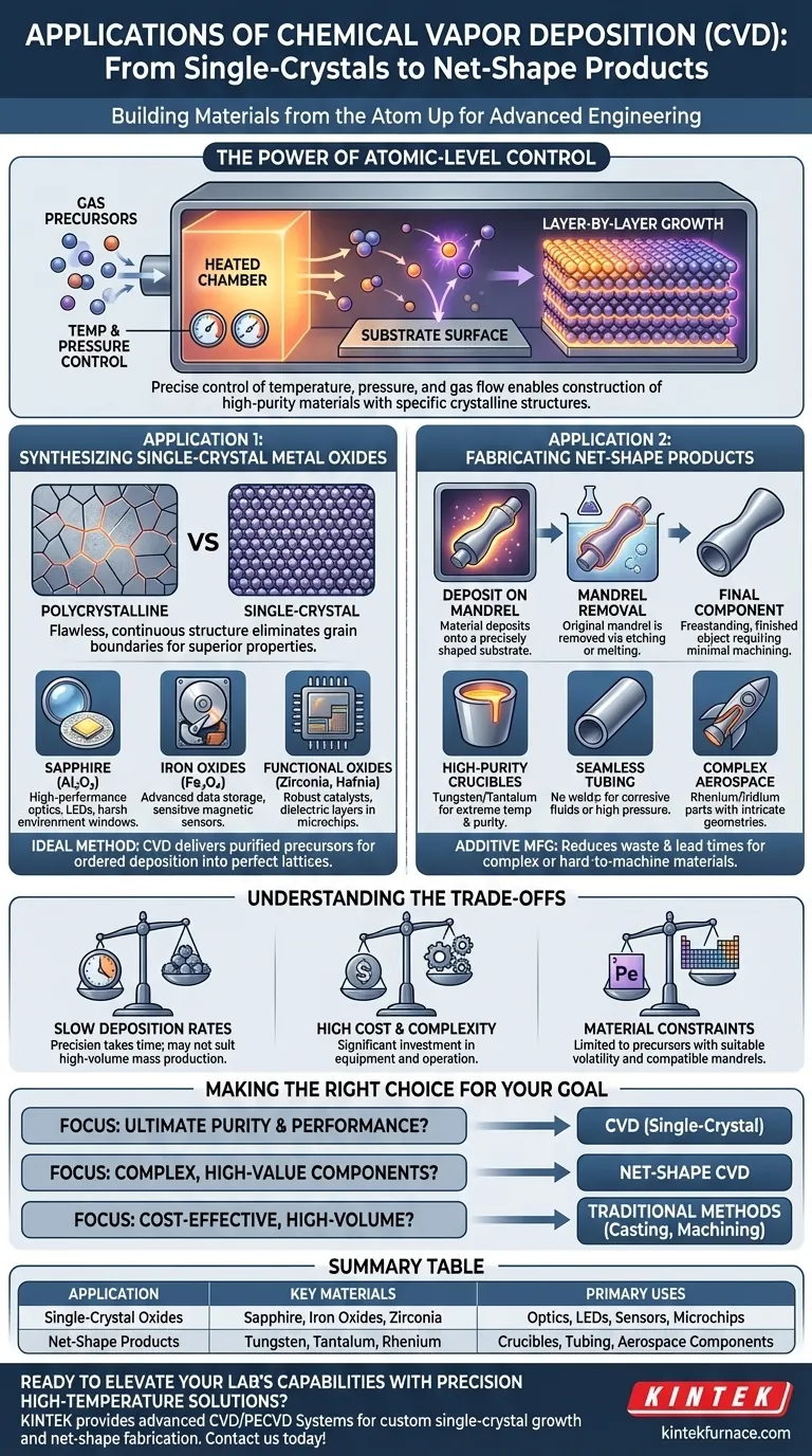
In short, Chemical Vapor Deposition (CVD) is used to synthesize ultra-pure single-crystal metal oxides like sapphire for high-performance optoelectronic and magnetic systems. Simultaneously, it serves as an additive manufacturing technique to create complex, finished components—known as net-shape products—such as tubes and crucibles with minimal material waste.
CVD is not merely a coating technology; it is a foundational manufacturing process. It gives engineers the power to construct materials from the atom up, enabling the creation of both fundamentally perfect crystalline structures and functionally complete, complex objects.
The Power of Atomic-Level Control
Chemical Vapor Deposition is a process where volatile chemical precursors react or decompose on a heated substrate surface to deposit a solid material. This layer-by-layer growth is the key to its unique capabilities.
By precisely controlling temperature, pressure, and gas flow, CVD allows for the construction of materials with exceptionally high purity and specific crystalline structures, a level of control that traditional metallurgical or ceramic processes cannot match.
Application 1: Synthesizing Single-Crystal Metal Oxides
The flawless, repeating atomic structure of a single crystal gives it predictable and superior properties compared to its polycrystalline counterparts.
What is a Single-Crystal Oxide?
A single-crystal material is one where the entire solid consists of a single, continuous, and unbroken crystal lattice. This eliminates grain boundaries, which are defects that can scatter light, impede electrical current, or serve as points of chemical and mechanical failure.
Key Materials and Their Uses
CVD is the preferred method for growing high-purity oxide crystals for demanding applications.
- Sapphire (Al₂O₃): As a single crystal, it is transparent from deep UV to mid-infrared wavelengths, making it ideal for high-performance lenses, windows in harsh environments, and as a substrate for manufacturing LEDs.
- Iron Oxides (e.g., Fe₃O₄): The ability to grow pure, structured films of magnetic oxides is critical for advanced data storage systems and sensitive magnetic field sensors.
- Other Functional Oxides (e.g., Zirconia, Hafnia): These materials are grown via CVD for use as robust catalysts in the chemical industry or as high-performance dielectric layers in next-generation microchips.
Why CVD is the Ideal Method
Growing a perfect crystal requires an environment free of impurities and a slow, ordered deposition process. CVD provides this by delivering purified chemical precursors directly to the growth surface, allowing atoms to arrange themselves into the lowest-energy state: a perfect crystal lattice.
Application 2: Fabricating Net-Shape Products
Beyond films and crystals, CVD is used to build entire three-dimensional objects in their final, or "net," shape. This is a form of additive manufacturing that excels where traditional methods fail.
Defining "Net-Shape" Manufacturing
Net-shape manufacturing aims to produce a component that requires little to no finishing work, like machining or grinding. This drastically reduces material waste, lead times, and costs, especially for complex or hard-to-machine materials.
The CVD Process for Net-Shape
The technique involves depositing the desired material onto a precisely shaped mandrel or substrate. Once the deposition reaches the target thickness, the original mandrel is removed, typically by chemical etching or melting, leaving a freestanding, hollow object.
Practical Examples
This method is used to create components that must perform in extreme environments.
- High-Purity Crucibles: Crucibles made from materials like tungsten or tantalum are used in semiconductor manufacturing and research because they can withstand extreme temperatures without contaminating the high-purity melts they contain.
- Seamless Tubing: CVD-produced tubing has no seams or welds, which are weak points. This makes it invaluable for transporting corrosive fluids or for use in high-pressure systems.
- Complex Aerospace Components: Components with intricate internal channels or non-machinable geometries, such as rocket nozzles made from rhenium or iridium, are often fabricated using this net-shape CVD process.
Understanding the Trade-offs
While powerful, CVD is not a universal solution. Its selection must be weighed against its inherent limitations.
Slow Deposition Rates
The same precision that makes CVD so effective also means it is often a slow process. For thick components or mass production, the time required can make it economically unviable compared to faster, conventional methods.
High Cost and Complexity
CVD reactors are complex systems that require vacuum chambers, high-temperature furnaces, and sophisticated gas handling for often-hazardous precursors. The initial capital investment and operational costs are significant.
Material and Substrate Constraints
The process is limited to materials that have suitable, volatile chemical precursors. Furthermore, the mandrel material must be compatible with the deposition temperature and easily removable without damaging the final product.
Making the Right Choice for Your Goal
Understanding when to leverage CVD is critical for any engineering project. Use these principles as your guide.
- If your primary focus is ultimate material purity and performance: CVD is the definitive choice for creating single-crystal materials where flawless structure dictates function, as in optics or advanced electronics.
- If your primary focus is manufacturing complex, high-value components: Use net-shape CVD for parts made from hard-to-machine materials or those with intricate geometries that are impossible to create with subtractive methods.
- If your primary focus is cost-effective, high-volume production: Carefully evaluate if the performance gains from CVD justify its higher cost and slower speed; traditional casting, forming, or machining may be more appropriate.
Ultimately, Chemical Vapor Deposition empowers you to build materials from first principles, achieving a level of structural perfection and product complexity that is otherwise unattainable.
Summary Table:
| Application | Key Materials | Primary Uses |
|---|---|---|
| Single-Crystal Metal Oxides | Sapphire (Al₂O₃), Iron Oxides (Fe₃O₄), Zirconia, Hafnia | High-performance optics, LEDs, magnetic sensors, catalysts, microchips |
| Net-Shape Products | Tungsten, Tantalum, Rhenium, Iridium | Crucibles, seamless tubing, aerospace components like rocket nozzles |
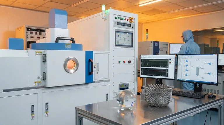
Ready to elevate your lab's capabilities with precision high-temperature solutions? KINTEK leverages exceptional R&D and in-house manufacturing to provide advanced furnaces like Muffle, Tube, Rotary, Vacuum & Atmosphere, and CVD/PECVD Systems. Our deep customization ensures they meet your unique needs for single-crystal growth or net-shape fabrication. Contact us today to discuss how our expertise can drive your innovations forward!
Visual Guide
Related Products
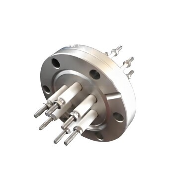
- Custom Made Versatile CVD Tube Furnace Chemical Vapor Deposition CVD Equipment Machine
- Multi Heating Zones CVD Tube Furnace Machine for Chemical Vapor Deposition Equipment
- HFCVD Machine System Equipment for Drawing Die Nano Diamond Coating
- Split Chamber CVD Tube Furnace with Vacuum Station CVD Machine
- 915MHz MPCVD Diamond Machine Microwave Plasma Chemical Vapor Deposition System Reactor
People Also Ask
- What future trends are expected in the development of CVD tube furnaces? Discover Smarter, More Versatile Systems
- How does CVD tube furnace sintering enhance graphene growth? Achieve Superior Crystallinity and High Electron Mobility
- What temperature range do standard CVD tube furnaces operate at? Unlock Precision for Your Material Deposition
- What improvements can be made to the bonding force of gate dielectric films using a CVD tube furnace? Enhance Adhesion for Reliable Devices
- What customization options are available for CVD tube furnaces? Tailor Your System for Superior Material Synthesis