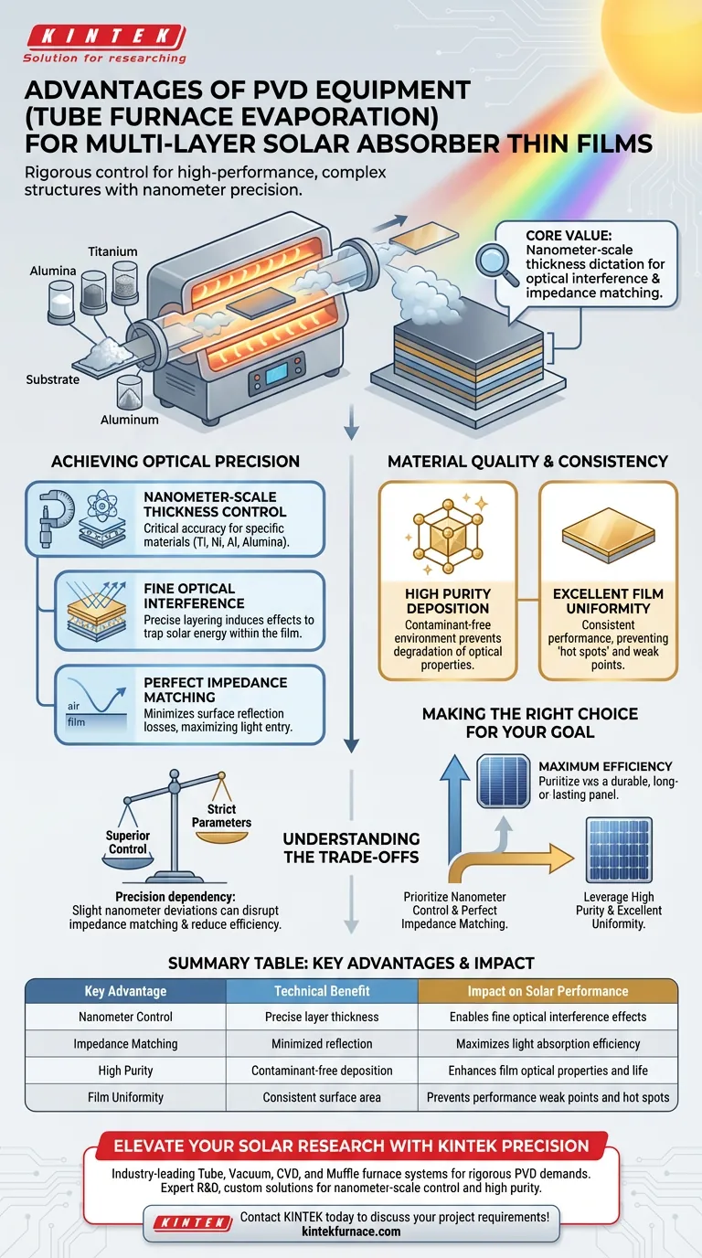
Physical vapor deposition (PVD) equipment, particularly tube furnace evaporation systems, provides the rigorous control necessary for fabricating high-performance solar absorber thin films. By delivering high purity and excellent film uniformity, these systems allow engineers to construct complex multi-layer structures using materials such as alumina, titanium, nickel, and aluminum with high precision.
The core value of this technology is its ability to dictate film thickness at the nanometer scale, which is the absolute prerequisite for creating fine optical interference effects and perfect impedance matching.
Achieving Optical Precision
Nanometer-Scale Thickness Control
The primary advantage of tube furnace evaporation systems is the ability to deposit layers with nanometer-level accuracy. This precision is critical when working with specific absorber materials like titanium, nickel, aluminum, and alumina.
Fine Optical Interference
Controlling thickness is not merely about structural dimensions; it is about manipulating light. Precise layering is required to induce specific optical interference effects that trap solar energy within the film.
Perfect Impedance Matching
To maximize absorption, the solar film must minimize reflection losses at the surface. PVD equipment enables the creation of structures that achieve perfect impedance matching, ensuring the maximum amount of light enters the absorber rather than bouncing off it.
Material Quality and Consistency
High Purity Deposition
Impurities in a thin film can degrade its optical properties and overall efficiency. PVD systems are designed to maintain high purity environments, ensuring that the deposited layers are free from contaminants that could hinder electron flow or light absorption.
Excellent Film Uniformity
Solar absorbers require consistent performance across the entire surface area of the device. Tube furnace evaporation systems deliver excellent film uniformity, preventing "hot spots" or weak points that can occur with less precise deposition methods.
Understanding the Trade-offs
The Necessity of Strict Parameters
While PVD systems offer superior control, this precision introduces a dependency on rigorous process parameters. Achieving the fine optical interference effects mentioned requires that the equipment be calibrated perfectly; even slight deviations in the nanometer scale can disrupt the impedance matching, significantly reducing the solar absorber's efficiency.
Making the Right Choice for Your Goal
To determine if this fabrication method aligns with your project requirements, consider your specific performance targets:
- If your primary focus is Maximum Efficiency: Prioritize this equipment for its ability to achieve perfect impedance matching through nanometer-scale thickness control.
- If your primary focus is Device Reliability: Leverage the high purity and excellent uniformity of PVD systems to ensure consistent performance across the entire solar absorber surface.
Precision in fabrication is the single most important factor in translating theoretical solar design into high-performance reality.
Summary Table:
| Key Advantage | Technical Benefit | Impact on Solar Performance |
|---|---|---|
| Nanometer Control | Precise layer thickness | Enables fine optical interference effects |
| Impedance Matching | Minimized reflection | Maximizes light absorption efficiency |
| High Purity | Contaminant-free deposition | Enhances film optical properties and life |
| Film Uniformity | Consistent surface area | Prevents performance weak points and hot spots |
Elevate Your Solar Research with KINTEK Precision
Don't let fabrication inconsistencies hinder your efficiency goals. KINTEK provides industry-leading Tube, Vacuum, CVD, and Muffle furnace systems specifically designed for the rigorous demands of PVD and thin-film deposition. Backed by expert R&D and specialized manufacturing, our systems offer the nanometer-scale control and high purity required to achieve perfect impedance matching for your solar absorbers. Whether you need a standard setup or a fully customizable solution tailored to your unique research needs, our team is ready to support your innovation.
Ready to achieve superior film uniformity? Contact KINTEK today to discuss your project requirements!
Visual Guide
References
- Cheng‐Fu Yang, Kuei‐Kuei Lai. Development and Fabrication of a Multi-Layer Planar Solar Light Absorber Achieving High Absorptivity and Ultra-Wideband Response from Visible Light to Infrared. DOI: 10.3390/nano14110930
This article is also based on technical information from Kintek Furnace Knowledge Base .
Related Products
- Slide PECVD Tube Furnace with Liquid Gasifier PECVD Machine
- Custom Made Versatile CVD Tube Furnace Chemical Vapor Deposition CVD Equipment Machine
- Inclined Rotary Plasma Enhanced Chemical Deposition PECVD Tube Furnace Machine
- Multi Heating Zones CVD Tube Furnace Machine for Chemical Vapor Deposition Equipment
- Inclined Rotary Plasma Enhanced Chemical Deposition PECVD Tube Furnace Machine
People Also Ask
- What is plasma in the context of PECVD? Unlock Low-Temperature Thin Film Deposition
- How does PECVD equipment contribute to TOPCon bottom cells? Mastering Hydrogenation for Maximum Solar Efficiency
- What are the disadvantages of tube furnace cracking when processing heavy raw materials? Avoid Costly Downtime and Inefficiency
- What are the typical conditions for plasma-enhanced CVD processes? Achieve Low-Temperature Thin Film Deposition
- What are the main advantages of PECVD tube furnaces compared to CVD tube furnaces? Lower Temp, Faster Deposition, and More


