At its core, the primary advantage of using an Inductively Coupled Plasma (ICP) source in PECVD is its ability to generate a very high-density plasma with low ion energy. This unique combination allows for rapid deposition of high-quality thin films with minimal substrate damage and contamination, making it superior for demanding, large-scale manufacturing applications.
The critical distinction is that ICP decouples the generation of plasma density from the energy of ions bombarding the substrate. This allows you to achieve high deposition rates without the collateral damage often associated with other plasma sources.
How ICP Achieves Superior Performance
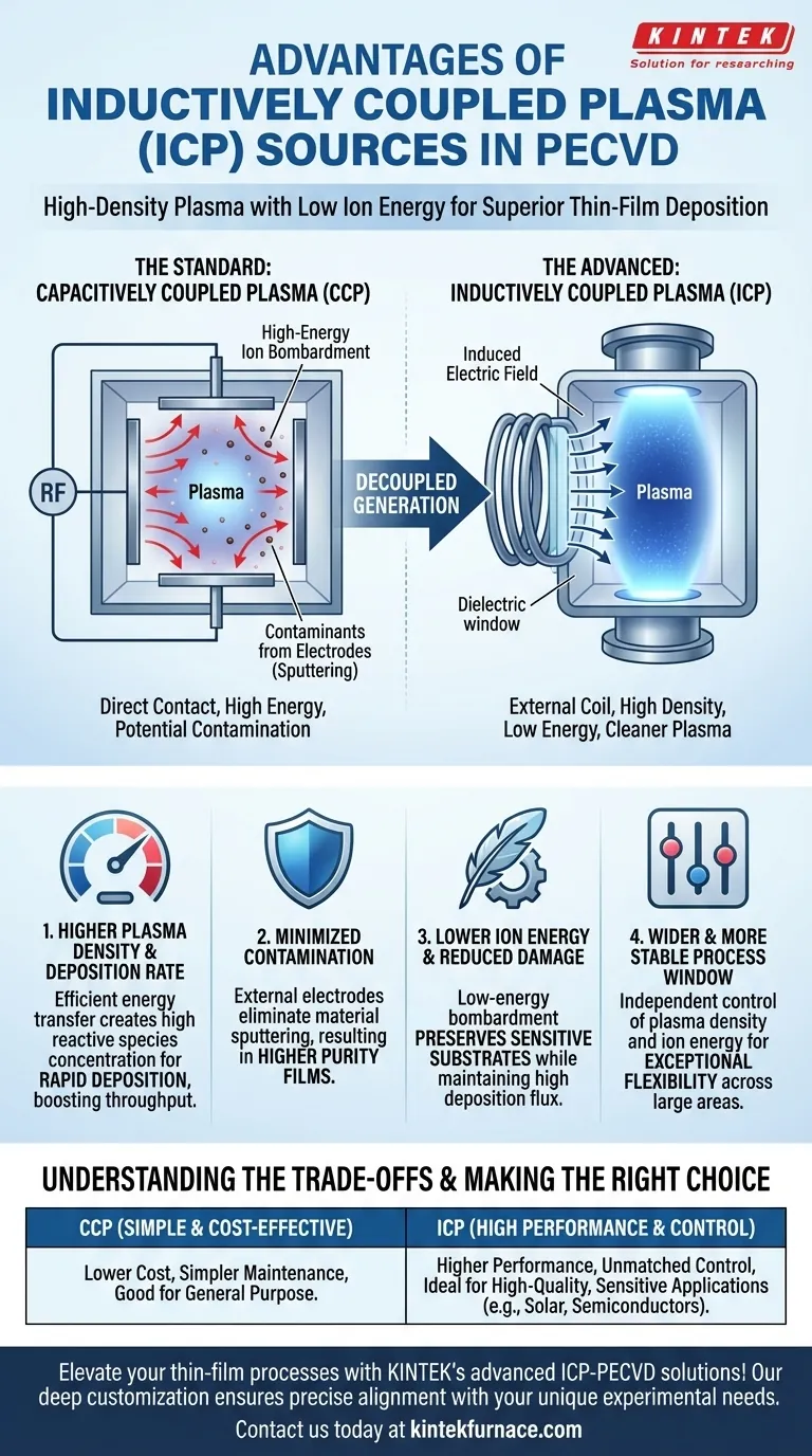
To understand the advantages of ICP, it is helpful to first contrast it with the more conventional Capacitively Coupled Plasma (CCP) method. Their fundamental difference in plasma generation is the source of ICP's benefits.
The Standard Method: Capacitively Coupled Plasma (CCP)
A CCP system uses two parallel metal electrodes inside the reaction chamber. One electrode is powered by a radio frequency (RF) source, and the other is grounded, creating an electric field between them that ignites and sustains the plasma.
While common and relatively simple, this design means the electrodes are in direct contact with the plasma.
The Advanced Method: Inductively Coupled Plasma (ICP)
An ICP system uses an external RF-powered coil wrapped around a dielectric portion of the chamber. This coil generates a time-varying magnetic field, which in turn induces a circular electric field inside the chamber.
This induced electric field accelerates electrons to ionize the gas and create a very dense plasma, all without any internal electrodes.
Key Advantages of the ICP Approach
The unique design of an ICP source directly translates into four significant process advantages for PECVD.
1. Higher Plasma Density and Deposition Rate
ICP's electromagnetic induction is far more efficient at transferring energy into the plasma than the direct fields of a CCP. This creates a much higher density of electrons and reactive species (radicals, ions).
This high concentration of reactive precursors leads to significantly higher dissociation and, consequently, much faster thin-film deposition rates, which is critical for high-throughput manufacturing.
2. Minimized Contamination for Higher Purity
In a CCP system, the internal electrodes are constantly bombarded by energetic ions from the plasma. This can cause the electrode material to sputter or erode, introducing metallic contaminants into the chamber and the deposited film.
Because ICP sources have their electrodes outside the reaction chamber, this entire contamination pathway is eliminated. The result is a cleaner plasma and higher-purity films.
3. Lower Ion Energy and Reduced Substrate Damage
High-density plasma in a CCP system often requires high voltages, leading to high-energy ion bombardment on the substrate surface. This can cause significant damage, especially for sensitive electronic materials.
ICP generates a high-density plasma at low pressure with a much lower plasma potential. This results in low-energy ion bombardment, preserving the delicate structure of the substrate while still benefiting from a high flux of reactive species for deposition.
4. Wider and More Stable Process Window
The ability to independently control plasma density (via ICP power) and ion energy (often via a separate RF bias on the substrate holder) gives ICP systems exceptional flexibility.
This decoupling allows engineers to fine-tune the deposition process for specific film properties, achieving exceptional layer quality across a wide range of operating conditions and over very large substrate areas.
Understanding the Trade-offs
While powerful, ICP is not always the necessary choice. The decision between ICP and CCP involves clear trade-offs between performance and complexity.
Simplicity and Cost
CCP systems are mechanically simpler and generally less expensive to build and maintain. Their straightforward design makes them a workhorse for many general-purpose thin-film applications where ultimate purity or deposition rate is not the primary driver.
Performance and Control
ICP systems are more complex but offer a level of control and performance that CCP cannot match. The ability to produce high-quality films at high rates with minimal damage justifies the investment for advanced applications like high-efficiency solar cells or next-generation semiconductors.
Making the Right Choice for Your Application
Your choice of plasma source should be dictated by the specific requirements of your thin film and the goals of your process.
- If your primary focus is high throughput and deposition rate: ICP is the superior choice due to its ability to generate extremely dense plasma.
- If your primary focus is film purity and processing sensitive substrates: ICP's external electrodes and low-energy ion bombardment provide an unmatched advantage.
- If your primary focus is cost-effectiveness for general-purpose films: A traditional CCP system is often the most practical and sufficient solution.
Ultimately, choosing an ICP source is an investment in achieving a higher ceiling for both the quality and the deposition speed of your thin films.
Summary Table:
| Advantage | Description |
|---|---|
| Higher Plasma Density & Deposition Rate | Enables faster thin-film deposition due to efficient energy transfer and high reactive species concentration. |
| Minimized Contamination | External electrodes eliminate material sputtering, ensuring higher purity films. |
| Lower Ion Energy & Reduced Substrate Damage | Low-energy ion bombardment preserves sensitive substrates while maintaining high deposition rates. |
| Wider Process Window | Independent control of plasma density and ion energy allows fine-tuning for various film properties and large areas. |
Elevate your thin-film processes with KINTEK's advanced high-temperature furnace solutions! Leveraging exceptional R&D and in-house manufacturing, we provide diverse laboratories with tailored ICP-PECVD systems, including our CVD/PECVD Systems, designed for high-density plasma and minimal substrate damage. Our strong deep customization capability ensures precise alignment with your unique experimental needs, whether for semiconductors, solar cells, or other demanding applications. Contact us today to discuss how our solutions can enhance your deposition rates and film quality!
Visual Guide
Related Products
- Slide PECVD Tube Furnace with Liquid Gasifier PECVD Machine
- Inclined Rotary Plasma Enhanced Chemical Deposition PECVD Tube Furnace Machine
- Inclined Rotary Plasma Enhanced Chemical Deposition PECVD Tube Furnace Machine
- RF PECVD System Radio Frequency Plasma Enhanced Chemical Vapor Deposition
- MPCVD Machine System Reactor Bell-jar Resonator for Lab and Diamond Growth
People Also Ask
- What are the disadvantages of tube furnace cracking when processing heavy raw materials? Avoid Costly Downtime and Inefficiency
- How does PECVD equipment contribute to TOPCon bottom cells? Mastering Hydrogenation for Maximum Solar Efficiency
- What are the typical conditions for plasma-enhanced CVD processes? Achieve Low-Temperature Thin Film Deposition
- What are the main advantages of PECVD tube furnaces compared to CVD tube furnaces? Lower Temp, Faster Deposition, and More
- In which industries is the tube furnace commonly used? Essential for Materials Science, Energy, and More


