At its core, Chemical Vapor Deposition (CVD) is a foundational manufacturing process used to create high-performance thin films and coatings. It is instrumental across a vast range of industries, including semiconductor fabrication, aerospace engineering, biomedical devices, and renewable energy, where modifying a material's surface properties is critical for function and durability.
The true value of CVD isn't just its wide range of applications, but its fundamental ability to engineer material surfaces atom-by-atom. This allows industries to create ultra-thin, highly pure, and durable films that grant ordinary materials extraordinary properties like conductivity, heat resistance, or biocompatibility.
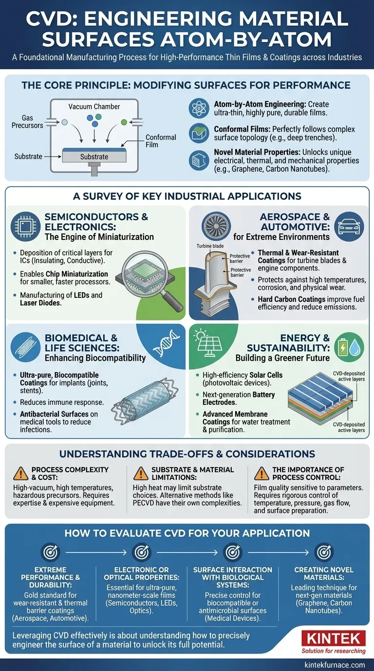
The Core Principle: Modifying Surfaces for Performance
What is Chemical Vapor Deposition?
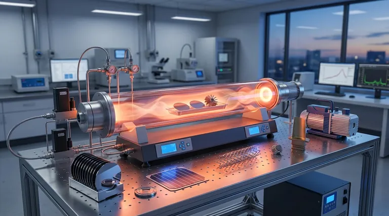
CVD is a process where a substrate (the part to be coated) is exposed to one or more volatile chemical precursors in a vacuum chamber. These precursors react and/or decompose on the substrate's surface to produce the desired solid deposit, or film.
This technique is not simply applying a layer of paint; it is building a new, solid material layer directly onto a surface from a gas phase. This provides an exceptional level of control over the film's thickness, purity, and structure.
The Power of Conformal Films
One of CVD's most significant advantages is its ability to create conformal films. This means the coating perfectly follows the surface topology of the substrate, covering complex, three-dimensional shapes with a uniform thickness.
This capability is essential for applications like microelectronics, where circuits have intricate patterns with deep trenches and high walls that must be coated evenly.
Unlocking Novel Material Properties
CVD is used to deposit a vast library of materials, including metals, ceramics, and polymers. It is also a key method for synthesizing advanced materials like graphene and carbon nanotubes.
By precisely controlling the deposition process, engineers can create films with unique and highly desirable electrical, thermal, or mechanical properties that the underlying substrate material does not possess.
A Survey of Key Industrial Applications
Semiconductors and Electronics: The Engine of Miniaturization
The modern electronics industry is built on CVD. It is used to deposit the critical layers that make up integrated circuits, from silicon nitride insulating layers to conductive films.
This precise deposition is what enables chip miniaturization, allowing for the creation of smaller, faster, and more powerful processors. CVD is also essential for manufacturing optoelectronics like LEDs and laser diodes.
Aerospace and Automotive: Engineering for Extreme Environments
In the aerospace and automotive industries, components must withstand extreme conditions. CVD is used to apply thermal and wear-resistant coatings to parts like jet engine turbine blades and automotive engine components.
These coatings protect the underlying metal from high temperatures, corrosion, and physical wear. In cars, specialized hard carbon coatings on fuel injection systems improve durability, increase fuel efficiency, and help reduce emissions.
Biomedical and Life Sciences: Enhancing Biocompatibility
When a device is implanted in the human body, its surface must not provoke an immune response. CVD is used to apply ultra-pure, biocompatible coatings to medical implants like artificial joints and stents.
This process can also be used to create antibacterial surfaces on medical tools, reducing the risk of hospital-acquired infections.
Energy and Sustainability: Building a Greener Future
CVD plays a vital role in renewable energy. It is a key step in manufacturing high-efficiency solar cells (photovoltaic devices) and developing next-generation battery electrodes.
Beyond energy generation, specialized CVD processes are used to create advanced membrane coatings for industrial water treatment and purification.
Understanding the Trade-offs and Considerations
Process Complexity and Cost
CVD is not a simple process. It typically requires high-vacuum environments, high temperatures, and the handling of volatile and sometimes hazardous precursor gases.
This complexity means that CVD equipment can be expensive, and the process requires significant expertise to optimize and control.
Substrate and Material Limitations
The high temperatures involved in many conventional CVD processes limit the types of substrates that can be coated. Materials with low melting points or those that are sensitive to thermal stress may not be suitable.
While lower-temperature CVD variations exist (e.g., Plasma-Enhanced CVD), they come with their own set of complexities and trade-offs.
The Importance of Process Control
The quality of a CVD film is highly sensitive to process parameters. Small fluctuations in temperature, pressure, or gas flow can dramatically alter the final material's properties.
Success requires rigorous control and optimization of factors like part fixturing, surface preparation, and gas chemistry to achieve consistent, high-quality results.
How to Evaluate CVD for Your Application
Choosing the right surface modification technology depends entirely on your end goal. CVD is a powerful but specialized tool.
- If your primary focus is extreme performance and durability: CVD is the gold standard for creating the wear-resistant and thermal barrier coatings required in aerospace and high-performance automotive parts.
- If your primary focus is electronic or optical properties: CVD is essential for depositing the ultra-pure, nanometer-scale thin films required for modern semiconductors, LEDs, and advanced optics.
- If your primary focus is surface interaction with biological systems: CVD provides the precise control needed to create the highly biocompatible or antimicrobial surfaces essential for advanced medical devices.
- If your primary focus is creating novel materials: CVD is a leading technique for synthesizing next-generation materials like graphene and carbon nanotubes at a commercially relevant scale.
Ultimately, leveraging CVD effectively is about understanding how to precisely engineer the surface of a material to unlock its full potential.
Summary Table:
| Industry | Key CVD Applications | Benefits |
|---|---|---|
| Semiconductors & Electronics | Deposition of insulating layers, conductive films for ICs, LEDs, and laser diodes | Enables miniaturization, improves performance and purity |
| Aerospace & Automotive | Thermal and wear-resistant coatings for turbine blades, engine parts | Enhances durability, heat resistance, and reduces emissions |
| Biomedical & Life Sciences | Biocompatible coatings on implants, antibacterial surfaces on tools | Improves biocompatibility, reduces infection risks |
| Energy & Sustainability | Manufacturing solar cells, battery electrodes, water treatment membranes | Boosts efficiency in renewable energy and purification systems |
Ready to engineer superior materials with advanced CVD solutions? At KINTEK, we leverage exceptional R&D and in-house manufacturing to provide diverse laboratories with cutting-edge high-temperature furnace solutions. Our product line, including Muffle, Tube, Rotary Furnaces, Vacuum & Atmosphere Furnaces, and CVD/PECVD Systems, is complemented by strong deep customization capabilities to precisely meet your unique experimental requirements. Whether you're in semiconductors, aerospace, biomedical, or energy, our expertise ensures optimal performance and durability for your applications. Contact us today to discuss how we can tailor our solutions to your needs and unlock the full potential of your materials!
Visual Guide
Related Products
- Custom Made Versatile CVD Tube Furnace Chemical Vapor Deposition CVD Equipment Machine
- Multi Heating Zones CVD Tube Furnace Machine for Chemical Vapor Deposition Equipment
- HFCVD Machine System Equipment for Drawing Die Nano Diamond Coating
- Split Chamber CVD Tube Furnace with Vacuum Station CVD Machine
- 915MHz MPCVD Diamond Machine Microwave Plasma Chemical Vapor Deposition System Reactor
People Also Ask
- What is a CVD tube furnace and what is its primary function? Discover Precision Thin-Film Deposition
- What customization options are available for CVD tube furnaces? Tailor Your System for Superior Material Synthesis
- What is the working principle of a CVD tube furnace? Achieve Precise Thin Film Deposition for Your Lab
- How might AI and machine learning enhance CVD tube furnace processes? Boost Quality, Speed, and Safety
- What are the key features of CVD tube furnaces for 2D material processing? Unlock Precision Synthesis for Superior Materials


