In solar cell manufacturing, Chemical Vapor Deposition (CVD) is a foundational technology used to deposit the ultra-thin, high-performance films that are essential for a cell to function. These precisely engineered layers perform distinct tasks, from converting sunlight into electricity to maximizing light absorption and protecting the cell, making CVD critical for achieving high energy conversion efficiency.
Manufacturing an efficient solar cell is a game of nanometers where every layer must be perfect. CVD provides the atomic-level control needed to build the cell's most critical components, making it an indispensable process for producing high-performance, cost-effective photovoltaic devices.
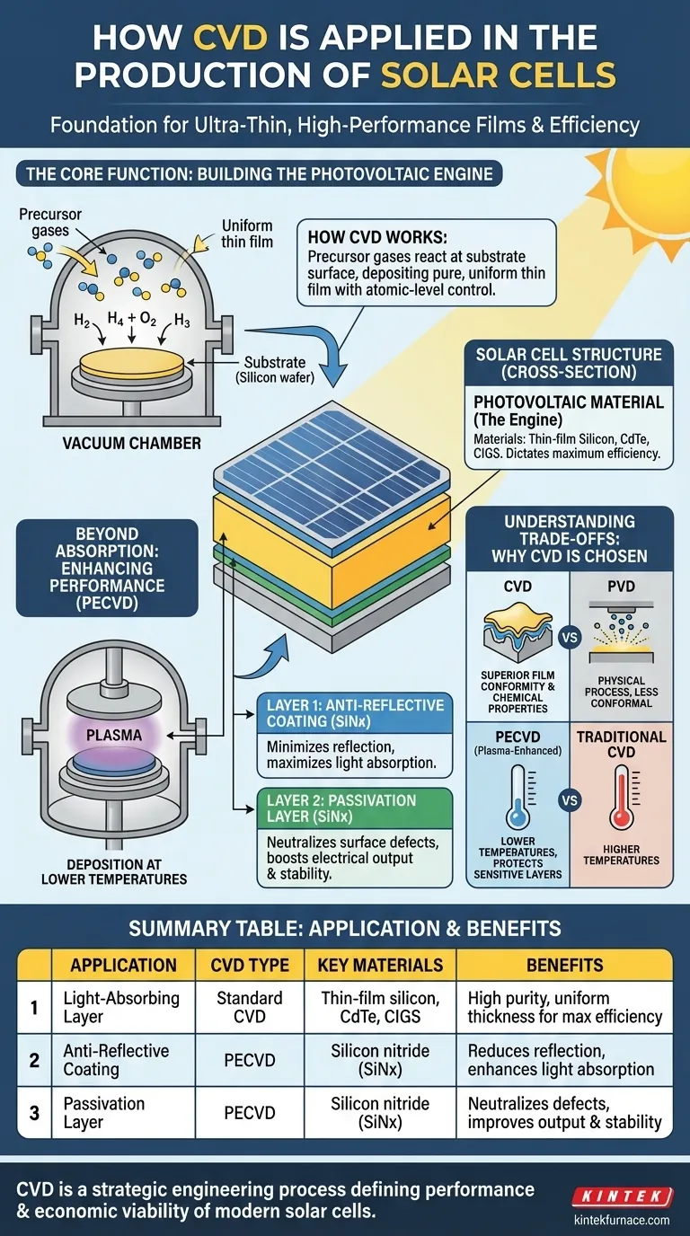
The Core Function: Building the Photovoltaic Engine
The primary role of CVD in solar cell production is to construct the material layers that form the heart of the device. This is not merely a coating process but a highly controlled method of fabrication.
How CVD Works at a High Level
At its core, CVD involves introducing precursor gases into a vacuum chamber containing the substrate (such as a silicon wafer). These gases react chemically at the surface of the substrate, depositing a solid, thin film.
This process is valued for its ability to create exceptionally pure and uniform layers, where thickness and chemical composition can be controlled with extreme precision.
Depositing the Light-Absorbing Layer
The most fundamental layer is the photovoltaic material itself—the active "engine" that absorbs photons from sunlight and releases electrons.
CVD is used to deposit key photovoltaic materials, including:
- Thin-film silicon
- Cadmium Telluride (CdTe)
- Copper Indium Gallium Selenide (CIGS)
The quality and uniformity of this layer directly dictate the maximum possible efficiency of the solar cell.
Beyond Absorption: Enhancing Performance and Durability
While the photovoltaic layer is key, a modern solar cell requires additional layers to reach peak performance. CVD, particularly a variant called Plasma-Enhanced CVD (PECVD), is used to apply these crucial finishing layers.
Layer 1: The Anti-Reflective Coating
A bare silicon wafer is naturally shiny and reflects a significant portion of incoming sunlight. To maximize energy generation, this reflection must be minimized.
PECVD is used to deposit a thin film of silicon nitride (SiNx) on the cell's surface. This film is optically engineered to reduce reflection, allowing more light to enter the photovoltaic material and be converted into electricity.
Layer 2: The Passivation Layer
Microscopic imperfections and "dangling bonds" naturally exist on the surface of a silicon wafer. These defects can trap the electrons released by sunlight, preventing them from being collected as electrical current and thus reducing efficiency.
The same silicon nitride film that serves as an anti-reflective coating also performs a function called passivation. The film effectively neutralizes these surface defects, allowing charge carriers to move freely and significantly boosting the cell's overall electrical output and long-term stability.
Understanding the Trade-offs: Why CVD is Chosen
CVD is not the only thin-film deposition technique, but its specific characteristics make it uniquely suited for the demands of solar cell manufacturing.
CVD vs. Physical Vapor Deposition (PVD)
PVD is another common deposition method, but it works through physical means (like sputtering) rather than a chemical reaction.
While PVD has its uses, CVD is often preferred for solar applications because it provides superior film conformity, meaning it can evenly coat complex surface topographies. More importantly, the chemical reaction process allows for the precise material properties, like those needed for passivation, that PVD cannot easily achieve.
The Importance of Process Variants like PECVD
"CVD" is a family of technologies. The use of Plasma-Enhanced CVD (PECVD) is a critical choice for depositing top layers like silicon nitride.
By using plasma, PECVD can run at much lower temperatures than traditional CVD. This is vital because high temperatures could damage the sensitive photovoltaic layers that have already been deposited on the wafer. PECVD allows for the addition of performance-enhancing films without compromising the cell's core structure.
How to Apply This to Your Goal
The specific application of CVD in your process depends directly on the manufacturing objective.
- If your primary focus is creating the core light-absorbing layer: You will use CVD to deposit materials like thin-film silicon or CdTe, where controlling film purity and uniform thickness is the top priority.
- If your primary focus is maximizing light absorption and efficiency: You will use Plasma-Enhanced CVD (PECVD) to apply a precisely calibrated silicon nitride anti-reflective coating.
- If your primary focus is improving electrical performance and longevity: The passivation properties of the PECVD-deposited silicon nitride film are crucial for neutralizing surface defects and protecting the cell.
Ultimately, CVD is not just a coating step; it is a strategic engineering process that directly defines the performance and economic viability of modern solar cells.
Summary Table:
| Application | CVD Type | Key Materials | Benefits |
|---|---|---|---|
| Light-Absorbing Layer | Standard CVD | Thin-film silicon, CdTe, CIGS | High purity, uniform thickness for maximum efficiency |
| Anti-Reflective Coating | PECVD | Silicon nitride (SiNx) | Reduces reflection, enhances light absorption |
| Passivation Layer | PECVD | Silicon nitride (SiNx) | Neutralizes defects, improves electrical output and stability |
Ready to optimize your solar cell production with advanced CVD solutions? At KINTEK, we leverage exceptional R&D and in-house manufacturing to provide diverse laboratories with high-temperature furnace solutions, including CVD/PECVD systems. Our strong deep customization capability ensures we can precisely meet your unique experimental requirements for depositing ultra-thin, high-performance films. Contact us today to discuss how our tailored CVD technologies can enhance your efficiency and durability!
Visual Guide
Related Products
- HFCVD Machine System Equipment for Drawing Die Nano Diamond Coating
- Cylindrical Resonator MPCVD Machine System for Lab Diamond Growth
- Custom Made Versatile CVD Tube Furnace Chemical Vapor Deposition CVD Equipment Machine
- 915MHz MPCVD Diamond Machine Microwave Plasma Chemical Vapor Deposition System Reactor
- MPCVD Machine System Reactor Bell-jar Resonator for Lab and Diamond Growth
People Also Ask
- What is the advantage of using a CVD system for coating turbine blades? Master Complex Geometries with Ease
- What is chemical vapor deposition (CVD) and its primary industrial application? Unlock Precision Thin Films for Electronics
- What are the equipment for chemical vapor deposition? A Guide to the 5 Essential Components
- What role does Chemical Vapor Deposition (CVD) equipment play in the surface coating of carbon fibers for composites?
- What is the significance of the vacuum pressure control system in the CVD coating process for powders?