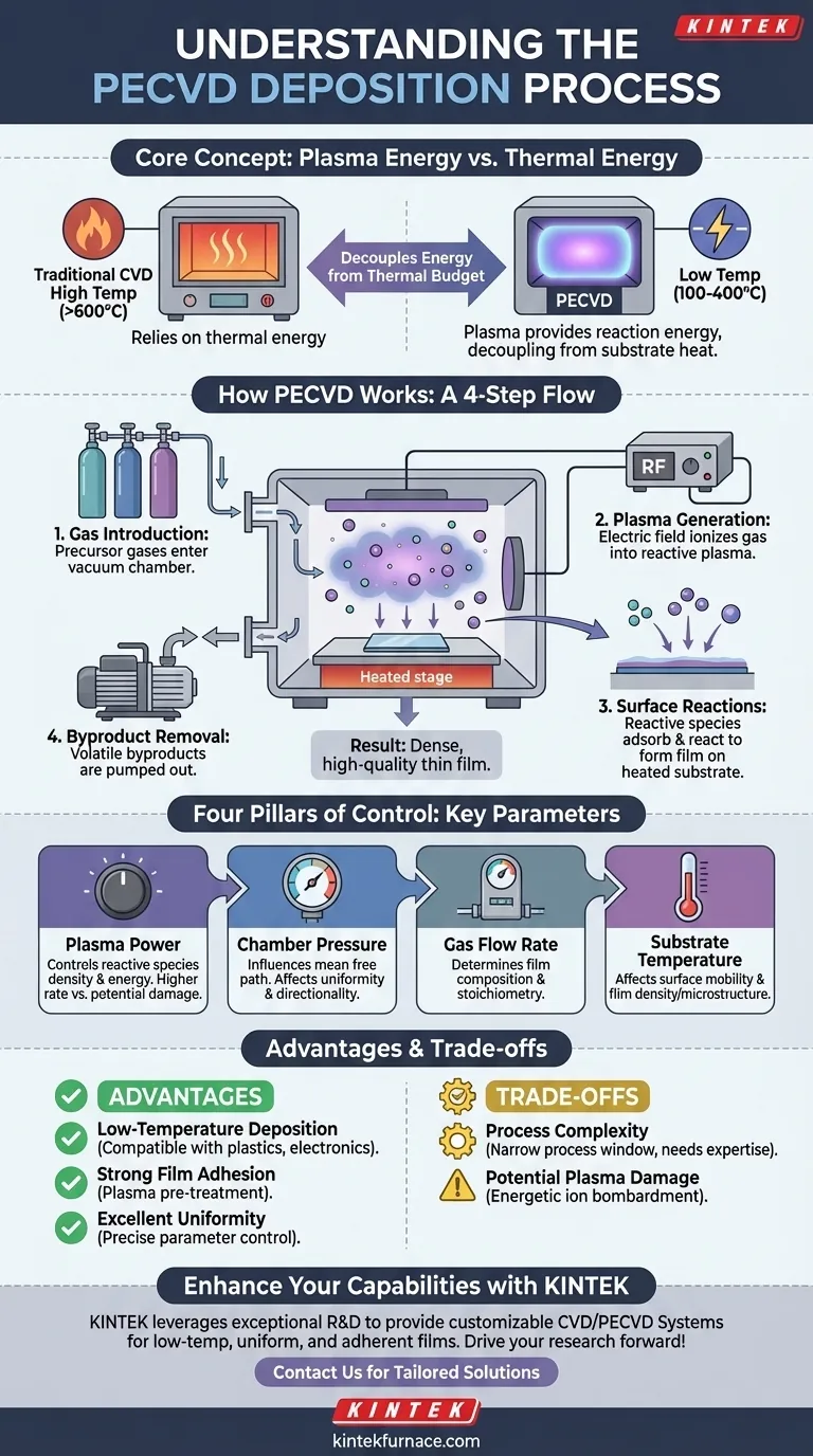
At its core, Plasma-Enhanced Chemical Vapor Deposition (PECVD) is a process that uses an energized plasma to deposit thin films onto a substrate. Unlike traditional Chemical Vapor Deposition (CVD) which relies on high temperatures to drive chemical reactions, PECVD uses an electric field to create a plasma, providing the necessary reaction energy at a much lower overall temperature. This allows high-quality films to be grown on materials that cannot withstand intense heat.
The central innovation of PECVD is its ability to decouple the energy required for chemical reactions from the thermal budget of the substrate. By using plasma instead of just heat, it enables the deposition of durable, uniform thin films at low temperatures, opening up applications for a wide range of sensitive materials.
How PECVD Works: A Step-by-Step Breakdown
The PECVD process occurs within a vacuum chamber and can be understood as a sequence of four distinct physical and chemical events.
Step 1: Gas Introduction and Chamber Preparation
First, the substrate (the material to be coated) is placed inside the reaction chamber. The chamber is then evacuated to a low base pressure.
Once the vacuum is established, a carefully controlled mixture of precursor gases is introduced. These gases contain the chemical elements required to form the final film.
Step 2: Plasma Generation - The Engine of the Process
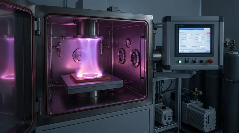
A high-frequency electric field (typically radio frequency or microwave) is applied to the gas inside the chamber. This powerful field ionizes the gas, stripping electrons from atoms and creating a plasma.
This plasma, often visible as a characteristic glow, is a highly reactive soup of ions, electrons, and neutral radicals. It is these activated species, not the original stable gas molecules, that will drive the deposition.
Step 3: Surface Reactions and Film Formation
The reactive species generated in the plasma diffuse toward the substrate, which is typically heated to a modest temperature (e.g., 100-400°C).
Upon reaching the surface, these species undergo chemical adsorption, sticking to the substrate and reacting with each other to form a solid, stable film. The substrate's temperature, while low, provides enough energy to promote surface mobility and ensure a dense, high-quality film structure.
Step 4: Byproduct Removal
The chemical reactions at the surface also create volatile byproducts. These byproducts desorb from the surface and are continuously removed from the chamber by the vacuum pumping system. This final step is critical for maintaining a pure deposition environment and achieving a high-purity film.
The Four Pillars of Control: Key Process Parameters
The quality, composition, and thickness of the deposited film are not accidental; they are dictated by precise control over four fundamental parameters.
### Plasma Power
This parameter directly controls the density and energy of the reactive species in the plasma. Higher power generally increases the deposition rate but can also introduce stress or cause plasma-induced damage to the substrate if not managed correctly.
### Chamber Pressure
Pressure influences the mean free path—the average distance a particle travels before colliding with another. Lower pressures result in fewer gas-phase collisions and more directional deposition, while higher pressures can increase deposition uniformity over complex topographies.
### Gas Flow Rate
The flow rate and ratio of different precursor gases determine the chemical makeup of the plasma and, consequently, the stoichiometry and composition of the final film. This allows for the deposition of complex materials like silicon nitride (SiNx) or silicon dioxide (SiO2).
### Substrate Temperature
While lower than in traditional CVD, the substrate temperature is still a critical lever. It affects the surface mobility of adsorbed species, influencing the film's density, stress, and microstructure. Higher temperatures generally lead to denser, more stable films.
Understanding the Advantages and Trade-offs
PECVD is a powerful technique, but its use requires a clear understanding of its benefits and inherent complexities.
### Advantage: Low-Temperature Deposition
This is the primary reason for choosing PECVD. Its ability to deposit films at low temperatures makes it compatible with temperature-sensitive substrates like plastics, polymers, and complex integrated circuits that would be damaged by high-heat processes.
### Advantage: Strong Film Adhesion
The plasma can be used to pre-treat or "clean" the substrate surface just before deposition begins. This removes contaminants and creates active bonding sites, resulting in exceptionally strong adhesion between the film and the substrate.
### Advantage: Excellent Uniformity
Precise, independent control over the four key process parameters allows engineers to fine-tune the reaction and transport conditions. This enables the growth of films with highly uniform thickness and composition across the entire surface of the substrate.
### Consideration: Process Complexity
Managing the interplay between pressure, power, gas flow, and temperature requires significant expertise. The process window for achieving a specific film property can be narrow, demanding sophisticated control systems and process development.
### Consideration: Potential for Plasma Damage
The energetic ions within the plasma, while essential for the reaction, can physically bombard and damage sensitive substrates or electronic devices. This effect must be carefully balanced by optimizing plasma power and chamber pressure.
Making the Right Choice for Your Application
Your specific goal will determine if PECVD is the appropriate technique for your project.
- If your primary focus is depositing on temperature-sensitive substrates: PECVD is the definitive choice because its plasma-based energy transfer avoids the need for destructive high temperatures.
- If your goal is a mechanically robust film with superior adhesion: The inherent plasma pre-treatment and energetic deposition of PECVD create a stronger film-substrate interface than many other methods.
- If you require precise control over film composition across a large area: The highly tunable parameters of PECVD allow for repeatable and uniform deposition, which is critical for manufacturing semiconductors and optical components.
Ultimately, PECVD's strength lies in its unique ability to deliver high-performance, engineered films in applications where high-temperature processes are simply not an option.
Summary Table:
| Step | Description | Key Outcome |
|---|---|---|
| 1. Gas Introduction | Precursor gases are introduced into a vacuum chamber. | Creates a controlled environment for deposition. |
| 2. Plasma Generation | Electric field ionizes gases to form a reactive plasma. | Generates activated species for chemical reactions. |
| 3. Surface Reactions | Reactive species adsorb and react on the heated substrate. | Forms a solid, dense thin film on the surface. |
| 4. Byproduct Removal | Volatile byproducts are removed via vacuum pumping. | Ensures high-purity and stable film deposition. |
| Parameter | Control Factor | Impact on Film |
| Plasma Power | Density and energy of reactive species. | Affects deposition rate and potential substrate damage. |
| Chamber Pressure | Mean free path of particles. | Influences deposition uniformity and directionality. |
| Gas Flow Rate | Stoichiometry and composition of the film. | Determines chemical makeup and film properties. |
| Substrate Temperature | Surface mobility and film microstructure. | Controls film density, stress, and stability. |
| Advantage | Benefit | Application Suitability |
| Low-Temperature Deposition | Compatible with heat-sensitive materials. | Ideal for plastics, polymers, and electronics. |
| Strong Film Adhesion | Plasma pre-treatment enhances bonding. | Suitable for durable coatings and interfaces. |
| Excellent Uniformity | Precise control over thickness and composition. | Essential for semiconductors and optics. |
Ready to enhance your laboratory's capabilities with advanced thin film deposition? KINTEK leverages exceptional R&D and in-house manufacturing to provide diverse laboratories with high-temperature furnace solutions, including CVD/PECVD Systems. Our strong deep customization capability ensures we precisely meet your unique experimental requirements for low-temperature, uniform, and adherent films. Contact us today to discuss how our tailored PECVD solutions can drive your research and production forward!
Visual Guide
Related Products
- RF PECVD System Radio Frequency Plasma Enhanced Chemical Vapor Deposition
- Inclined Rotary Plasma Enhanced Chemical Deposition PECVD Tube Furnace Machine
- Slide PECVD Tube Furnace with Liquid Gasifier PECVD Machine
- Inclined Rotary Plasma Enhanced Chemical Deposition PECVD Tube Furnace Machine
- 915MHz MPCVD Diamond Machine Microwave Plasma Chemical Vapor Deposition System Reactor
People Also Ask
- How is silicon dioxide deposited from tetraethylorthosilicate (TEOS) in PECVD? Achieve Low-Temperature, High-Quality SiO2 Films
- What is the role of RF power in PECVD and how does the RF-PECVD process work? Master Thin Film Deposition Control
- What are the advantages of PECVD in film deposition? Achieve Low-Temp, High-Quality Coatings
- What are the applications of plasma enhanced chemical vapor deposition? Key Uses in Electronics, Optics & Materials
- What is RF in PECVD? A Critical Control for Plasma Deposition


