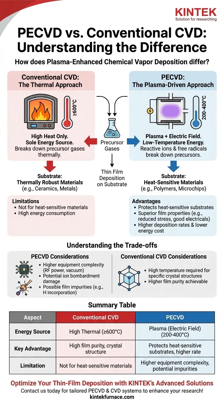
The fundamental difference between Plasma-Enhanced Chemical Vapor Deposition (PECVD) and conventional Chemical Vapor Deposition (CVD) is the source of energy used to drive the deposition reaction. While conventional CVD relies exclusively on high heat to break down precursor gases, PECVD utilizes an electric field to generate a plasma, allowing the reaction to occur at significantly lower temperatures.
By substituting the brute force of thermal energy with the targeted energy of a plasma, PECVD decouples the deposition process from high temperatures. This single change unlocks the ability to coat heat-sensitive materials that would be destroyed by conventional CVD methods.
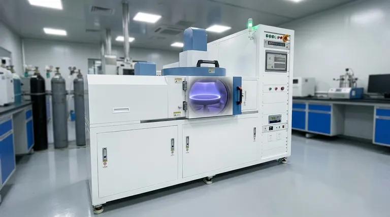
The Core Difference: How the Reaction is Activated
The goal of any CVD process is to break down gaseous chemical precursors so they react and deposit as a solid thin film onto a substrate. The key distinction lies in how that energy is supplied.
Conventional CVD: The Thermal Approach
Conventional, or thermal, CVD uses high temperatures, often well above 600°C, as the sole energy source. The substrate is heated in a chamber, and this thermal energy is what breaks the chemical bonds of the precursor gases flowing over it.
This method is conceptually simple but its high heat requirement makes it incompatible with many materials.
PECVD: The Plasma-Driven Approach
PECVD operates in a lower temperature range, typically 200–400°C. Instead of relying on heat alone, it introduces energy by applying an electric field to the gas, igniting a plasma.
This plasma is a highly energetic state of matter containing ions and free radicals. These reactive particles are what break down the precursor gases, enabling film deposition without needing extreme heat.
Key Advantages of Using Plasma
Lowering the process temperature via plasma creates several significant advantages that make PECVD a critical technology in modern manufacturing.
Protecting Temperature-Sensitive Substrates
This is the most significant advantage of PECVD. The lower operating temperature allows for the deposition of high-quality films on materials that cannot withstand high heat.
This includes polymers and plastics, as well as complex microelectronic devices where high temperatures could damage previously fabricated components or alter dopant profiles.
Achieving Superior Film Properties
The energetic-but-controlled nature of the plasma can lead to films with desirable characteristics. PECVD often produces films with reduced internal stress and a lower likelihood of cracking.
Furthermore, it can yield films with excellent electrical properties and strong adhesion to the substrate, critical for high-performance electronics and protective coatings.
Improving Deposition Rate and Efficiency
PECVD processes can often achieve higher deposition rates than their thermal CVD counterparts.
Because the system doesn't need to be heated to extreme temperatures, it also consumes significantly less energy, which can lead to lower production costs and higher throughput.
Understanding the Trade-offs
While powerful, the use of plasma is not without its considerations. Choosing between PECVD and conventional CVD involves understanding their respective limitations.
Process and Equipment Complexity
A PECVD system is inherently more complex than a thermal CVD reactor. It requires sophisticated RF power supplies to generate and sustain the plasma, along with advanced vacuum and gas control systems.
This added complexity can translate into higher initial equipment costs and more intricate process control.
Potential for Film Impurities or Damage
The high-energy ions within the plasma, while useful for the reaction, can sometimes cause ion bombardment damage to the substrate surface.
Additionally, precursor gases (like silane, SiH₄) can lead to the incorporation of other elements (like hydrogen) into the film. While sometimes beneficial, this can be an undesirable impurity in certain optical or electronic applications where film purity is paramount.
When High Temperature is a Feature, Not a Bug
For some materials, particularly certain crystalline structures, the high temperature of conventional CVD is not a drawback but a requirement. The thermal energy is necessary to achieve the desired crystal orientation and film density.
In these specific cases, the "gentler" PECVD process may not be able to produce a film with the required structural properties.
Making the Right Choice for Your Goal
Your choice depends entirely on the specific requirements of your substrate material and the desired properties of the final film.
- If your primary focus is depositing on heat-sensitive materials (like polymers or completed microchips): PECVD is the definitive choice due to its low-temperature process.
- If your primary focus is achieving the highest possible film purity or a specific crystal structure on a thermally robust substrate: Conventional thermal CVD may be preferable as it avoids potential plasma-induced effects.
- If your primary focus is balancing production speed, cost, and film quality for general-purpose coatings: PECVD often provides a superior balance of high deposition rates and excellent film properties at a lower energy cost.
Understanding this core trade-off between thermal and plasma energy empowers you to select the precise deposition technique your material requires.
Summary Table:
| Aspect | Conventional CVD | PECVD |
|---|---|---|
| Energy Source | High thermal energy (≥600°C) | Plasma from electric field (200-400°C) |
| Temperature Range | High (≥600°C) | Low (200-400°C) |
| Key Advantages | High film purity, specific crystal structures | Protects heat-sensitive substrates, higher deposition rates, lower energy use |
| Limitations | Not suitable for heat-sensitive materials | Higher equipment complexity, potential for ion damage or impurities |
Optimize Your Thin-Film Deposition with KINTEK's Advanced Solutions
Are you working with heat-sensitive materials like polymers or microelectronics and need precise, low-temperature deposition? KINTEK leverages exceptional R&D and in-house manufacturing to provide diverse laboratories with advanced high-temperature furnace solutions, including our specialized CVD/PECVD Systems. Our product line—featuring Muffle, Tube, Rotary Furnaces, Vacuum & Atmosphere Furnaces, and more—is complemented by strong deep customization capabilities to precisely meet your unique experimental requirements.
Contact us today to discuss how our tailored PECVD and CVD systems can enhance your research, improve film quality, and boost efficiency!
Visual Guide
Related Products
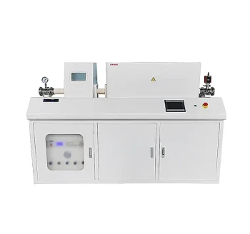
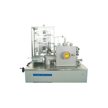
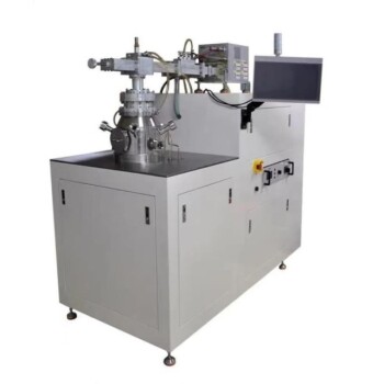
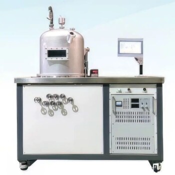
- RF PECVD System Radio Frequency Plasma Enhanced Chemical Vapor Deposition
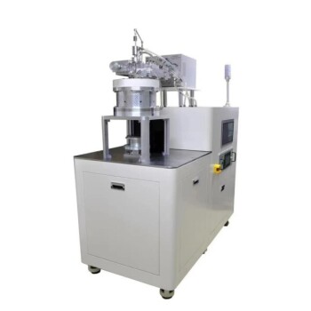
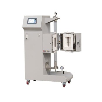
- Inclined Rotary Plasma Enhanced Chemical Deposition PECVD Tube Furnace Machine
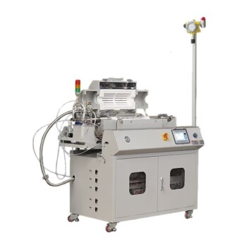
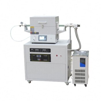
- Slide PECVD Tube Furnace with Liquid Gasifier PECVD Machine
- Inclined Rotary Plasma Enhanced Chemical Deposition PECVD Tube Furnace Machine
- Custom Made Versatile CVD Tube Furnace Chemical Vapor Deposition CVD Equipment Machine
People Also Ask
- What role does PECVD play in optical coatings? Essential for Low-Temp, High-Precision Film Deposition
- What is the second benefit of deposition within a discharge in PECVD? Enhance Film Quality with Ion Bombardment
- How does plasma vapor deposition work? A Low-Temperature Solution for Advanced Coatings
- What is PECVD equipment? A Guide to Low-Temperature Thin-Film Deposition
- What gases are used in the PECVD system? Optimize Thin Film Deposition with Precise Gas Selection


