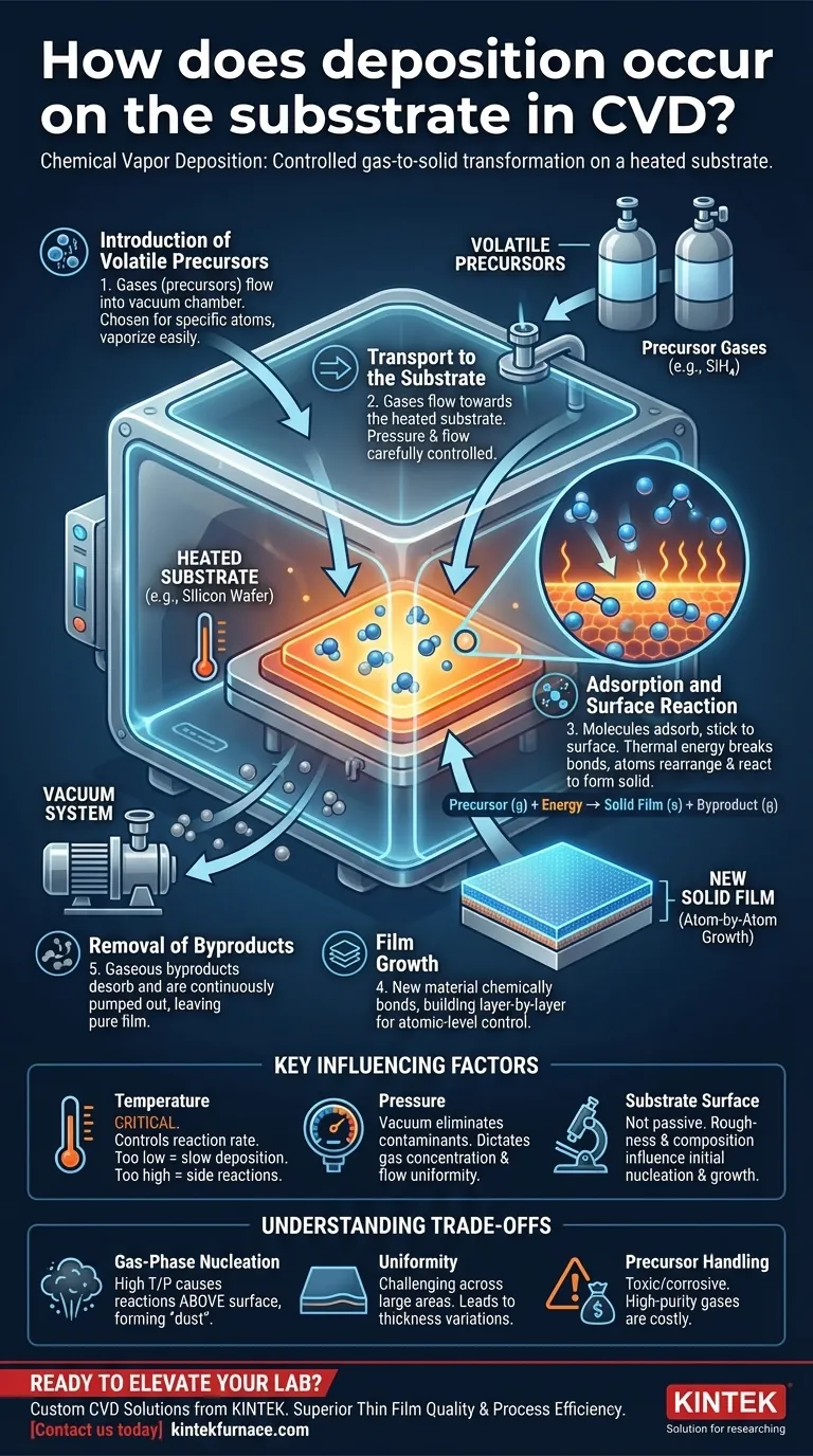
In Chemical Vapor Deposition (CVD), deposition occurs when volatile precursor gases are introduced into a vacuum chamber and react on a heated substrate. The thermal energy from the substrate breaks down these gas molecules, causing a chemical reaction that forms a new solid material. This solid material then deposits directly onto the substrate's surface, building up a thin film atom by atom or molecule by molecule.
The core principle of CVD is a controlled chemical transformation from a gas phase to a solid phase. This process is intentionally triggered by energy at a specific location—the substrate surface—allowing for the precise engineering of thin films with specific properties.
The Core Mechanism of CVD Deposition
To understand how deposition happens, it's best to view it as a sequence of carefully controlled steps. Each step is critical for determining the final quality, thickness, and uniformity of the deposited film.
1. Introduction of Volatile Precursors
The process begins by introducing one or more volatile precursor gases into a reaction chamber, which is held under a vacuum. These precursors are chemical compounds chosen because they contain the specific atoms needed for the final film and vaporize easily.
For example, to deposit solid silicon (Si), silane gas (SiH₄) might be used as a precursor.
2. Transport to the Substrate
Once inside the chamber, these precursor gases flow towards the substrate. The pressure and gas flow rates are meticulously controlled to ensure a stable and uniform supply of reactive molecules reaches the substrate surface.
3. Adsorption and Surface Reaction
When the precursor gas molecules arrive at the heated substrate, they adsorb, or temporarily stick, to its surface. The thermal energy from the substrate provides the activation energy needed to initiate a chemical reaction.
This energy breaks the chemical bonds in the precursor molecules. The constituent atoms then rearrange and react on the surface to form a stable, solid material.
4. Film Growth
The newly formed solid material is now part of the film, chemically bonded to the substrate or the previously deposited layer. This process repeats continuously, with more gas molecules adsorbing and reacting, building the film in a layer-by-layer manner.
This atomic-level control is what allows CVD to produce extremely thin, dense, and uniform coatings.
5. Removal of Byproducts
The chemical reactions that form the solid film also create gaseous byproducts. These byproduct gases desorb from the substrate surface and are continuously pumped out of the chamber by the vacuum system.
For instance, in the reaction Metal Halide (g) → Metal (s) + Byproduct (g), the metal deposits as a solid while the byproduct gas is removed, leaving a pure film.
Key Factors Influencing Deposition
The success of the CVD process hinges on the precise control of several key parameters. Each one directly influences the chemical reactions and, therefore, the final film properties.
The Role of Temperature
Substrate temperature is arguably the most critical parameter. It directly controls the rate of the surface chemical reactions. Too low a temperature results in a slow or non-existent deposition, while too high a temperature can cause undesirable side reactions.
The Importance of Pressure
The process is performed under vacuum to eliminate contaminants like oxygen or water vapor that could interfere with the chemistry. The specific pressure also dictates the concentration of precursor gas and how it flows, affecting the uniformity of the final film.
The Substrate Surface
The substrate is not just a passive platform. Its surface roughness and chemical composition can influence how the initial atoms of the film nucleate and grow. A clean, smooth surface is essential for achieving a high-quality, uniform film.
Understanding the Trade-offs
While powerful, the CVD process is not without its challenges. Understanding these limitations is key to troubleshooting and optimizing the deposition process.
Gas-Phase Nucleation
If the temperature or pressure is too high, the precursor gases can react in the space above the substrate, not just on its surface. This is called gas-phase nucleation.
This process forms tiny solid particles or "dust" that then fall onto the substrate, resulting in a powdery, poorly adhered, and low-quality film instead of the desired dense, solid layer.
Uniformity Across Large Areas
Achieving a perfectly uniform temperature and precursor gas concentration across a large substrate is a significant engineering challenge. Any variations can lead to differences in film thickness and properties from one part of the substrate to another.
Precursor Handling and Cost
CVD precursors can be highly toxic, flammable, or corrosive, requiring specialized handling and safety systems. Furthermore, high-purity precursor gases can be a major cost driver for the overall process.
Making the Right Choice for Your Goal
Your approach to CVD should be dictated by the specific properties you need in your final film.
- If your primary focus is creating an ultra-pure, dense film: You must carefully balance temperature and pressure to ensure reactions happen exclusively on the substrate surface, avoiding gas-phase nucleation.
- If your primary focus is precise thickness control: Your top priorities are stable precursor gas flow rates and a highly uniform substrate temperature to guarantee a consistent deposition rate.
- If your primary focus is depositing a specific compound (e.g., a ceramic like TiN): Your critical choice is the set of precursors (e.g., TiCl₄ and NH₃) that will react to form the desired material at a manageable temperature.
By mastering these fundamental principles, you can leverage CVD to engineer advanced materials with properties tailored at the atomic scale.
Summary Table:
| Step | Description | Key Factors |
|---|---|---|
| 1. Introduction of Precursors | Volatile gases enter vacuum chamber | Precursor choice, purity |
| 2. Transport to Substrate | Gases flow to heated substrate | Pressure, flow rate control |
| 3. Adsorption and Reaction | Molecules adsorb and react on surface | Temperature, surface energy |
| 4. Film Growth | Solid material deposits layer by layer | Reaction rate, uniformity |
| 5. Removal of Byproducts | Gaseous byproducts pumped out | Vacuum system efficiency |
Ready to elevate your lab's capabilities with custom high-temperature furnace solutions? KINTEK leverages exceptional R&D and in-house manufacturing to provide advanced CVD systems, Muffle Furnaces, Tube Furnaces, Rotary Furnaces, Vacuum & Atmosphere Furnaces, and more. Our deep customization ensures precise alignment with your unique experimental needs, delivering superior thin film quality and process efficiency. Contact us today to discuss how we can support your research and production goals!
Visual Guide
Related Products
- Custom Made Versatile CVD Tube Furnace Chemical Vapor Deposition CVD Equipment Machine
- Split Chamber CVD Tube Furnace with Vacuum Station CVD Machine
- Multi Heating Zones CVD Tube Furnace Machine for Chemical Vapor Deposition Equipment
- Slide PECVD Tube Furnace with Liquid Gasifier PECVD Machine
- Inclined Rotary Plasma Enhanced Chemical Deposition PECVD Tube Furnace Machine
People Also Ask
- What is the working principle of a CVD tube furnace? Achieve Precise Thin Film Deposition for Your Lab
- What improvements can be made to the bonding force of gate dielectric films using a CVD tube furnace? Enhance Adhesion for Reliable Devices
- What are the key application fields of CVD tube furnaces? Unlock Precision in Thin-Film Synthesis
- What are the key features of CVD tube furnaces for 2D material processing? Unlock Precision Synthesis for Superior Materials
- How does CVD tube furnace sintering enhance graphene growth? Achieve Superior Crystallinity and High Electron Mobility


