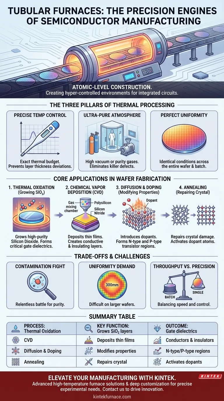
In semiconductor fabrication, tubular furnaces are not just heaters; they are precision instruments that create the hyper-controlled environments required for building integrated circuits. They are used for a few critical thermal processes: depositing ultra-thin films of material onto silicon wafers, growing high-purity oxide layers, and driving in or activating atoms to precisely modify the silicon's electrical properties.
At its core, fabricating a microchip is a process of atomic-level construction. Tubular furnaces provide the three non-negotiable conditions for this work: exceptionally precise temperature control, an ultra-pure processing atmosphere, and perfect heating uniformity across the entire wafer.
The Foundation: Why Thermal Processing is Critical
Thermal processing is a fundamental step in turning a blank silicon wafer into a functioning processor. Furnaces provide the energy needed to initiate and control specific chemical reactions and physical changes on the wafer's surface.
Building Circuits Atom by Atom
Modern circuits have features measured in nanometers. Creating these structures requires depositing perfect layers of material, often only a few atoms thick, and modifying the silicon crystal itself.
A tubular furnace provides the stable, predictable thermal budget—a combination of temperature and time—needed to ensure these processes happen correctly and repeatably for millions or billions of transistors on a single chip.
The Pillars: Temperature, Purity, and Uniformity
Temperature control must be exact. A deviation of even a few degrees can ruin a wafer by changing the thickness of a grown layer or the depth of diffused atoms, rendering the final devices useless.
Purity is paramount. These furnaces often operate under a high vacuum or are filled with specific, ultra-high-purity gases. Any unwanted particle or molecule can act as a "killer defect," short-circuiting a transistor and destroying the chip.
Uniformity ensures that every part of the wafer—and every wafer in a batch—experiences the exact same conditions. This guarantees that a transistor at the edge of the wafer behaves identically to one at the center.
Core Applications in Wafer Fabrication
Tubular furnaces are workhorses for several indispensable steps in the manufacturing flow. They are specialized for specific tasks, often referred to by the process they perform, such as a "diffusion furnace" or "CVD furnace."
Growing High-Purity Silicon Dioxide (Oxidation)
The process of thermal oxidation is used to grow a layer of silicon dioxide (SiO₂) on the wafer surface. This is achieved by heating the silicon wafer in an environment containing pure oxygen or water vapor.
This grown oxide is an exceptional electrical insulator, forming the critical "gate dielectric" in a transistor, which controls the flow of current.
Creating Insulating and Conductive Layers (Deposition)
Chemical Vapor Deposition (CVD) is a process where gases react within the furnace to form a solid film on the wafer's surface.
This technique is used to deposit various essential layers, such as polysilicon, which serves as a conductor for the transistor gate, and silicon nitride, which acts as a robust insulator or protective barrier.
Modifying Electrical Properties (Diffusion & Doping)
To create the N-type and P-type regions that form transistors, specific impurity atoms (dopants) must be introduced into the silicon crystal lattice.
Diffusion is a high-temperature process where wafers are heated in an atmosphere containing dopant gases. The heat gives the dopant atoms enough energy to move, or diffuse, into the silicon, changing its electrical characteristics in targeted areas.
Repairing and Activating the Crystal (Annealing)
After processes like ion implantation (where dopants are shot into the wafer), the silicon's crystal structure becomes damaged.
Annealing is a heat treatment process performed in a furnace that repairs this crystal damage. Critically, it also provides the energy needed to "activate" the dopant atoms, allowing them to become electrically integrated into the silicon lattice.
Understanding the Trade-offs and Challenges
While essential, using tubular furnaces presents significant engineering challenges that define the cutting edge of semiconductor manufacturing.
The Constant Fight Against Contamination
Maintaining purity is a relentless battle. The quartz tubes used in the furnaces, the gas delivery systems, and the wafer handling robotics must all be impeccably clean. Even the smallest leak or outgassing of material can introduce contaminants and devastate device yield.
The Demand for Absolute Uniformity
As wafers have grown larger (from 200mm to 300mm), ensuring the temperature is identical across a surface area the size of a dinner plate has become incredibly difficult. Sophisticated multi-zone heating elements and advanced control algorithms are required to achieve this.
Throughput vs. Precision
Batch furnaces, which process many wafers at once, offer high throughput but make achieving perfect uniformity for each wafer more challenging. Single-wafer rapid thermal processing (RTP) systems offer superior control but at a much lower throughput. Manufacturers must constantly balance this trade-off between speed and precision.
Making the Right Choice for Your Goal
The specific furnace process you use is dictated entirely by the layer or electrical characteristic you are trying to create on the wafer.
- If your primary focus is creating a pristine gate insulator: You will use thermal oxidation to grow a perfect silicon dioxide layer with minimal defects.
- If your primary focus is forming conductive paths or hard masks: You will rely on CVD to deposit films like polysilicon or silicon nitride.
- If your primary focus is defining the transistor's electrical behavior: You will use diffusion and annealing furnaces to introduce and activate dopants with extreme precision.
Ultimately, mastering these thermal processes is fundamental to turning a simple silicon wafer into a complex and powerful integrated circuit.
Summary Table:
| Process | Key Function | Materials/Outcomes |
|---|---|---|
| Thermal Oxidation | Grows silicon dioxide layers | Forms gate dielectrics for transistors |
| Chemical Vapor Deposition (CVD) | Deposits thin films | Creates conductive (polysilicon) and insulating (silicon nitride) layers |
| Diffusion & Doping | Modifies electrical properties | Introduces dopants to form N-type and P-type regions |
| Annealing | Repairs crystal damage | Activates dopants and restores silicon lattice integrity |
Elevate your semiconductor manufacturing with KINTEK's advanced high-temperature furnace solutions. Leveraging exceptional R&D and in-house manufacturing, we provide tubular furnaces and other systems like Muffle, Tube, Rotary, Vacuum & Atmosphere Furnaces, and CVD/PECVD Systems. Our deep customization capabilities ensure precise alignment with your unique experimental needs, enhancing yield and performance in thermal processes such as oxidation, deposition, and doping. Ready to optimize your lab's efficiency? Contact us today to discuss how our solutions can drive your innovation forward!
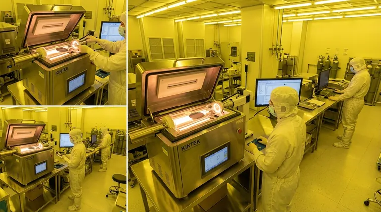
Visual Guide
Related Products
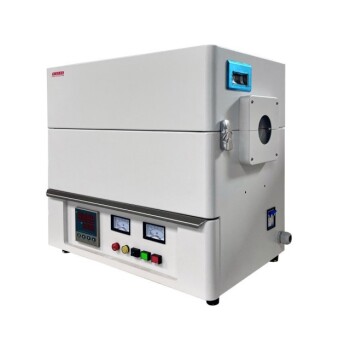
- Vertical Laboratory Quartz Tube Furnace Tubular Furnace
- Multi Zone Laboratory Quartz Tube Furnace Tubular Furnace
- High Pressure Laboratory Vacuum Tube Furnace Quartz Tubular Furnace
- Laboratory Quartz Tube Furnace RTP Heating Tubular Furnace
- 1700℃ High Temperature Laboratory Tube Furnace with Alumina Tube
People Also Ask
- Why is a vertical tube furnace preferred for quenching tests? Achieve Rapid, Repeatable Cooling for Accurate Results
- How do heat treatment processes influence the configuration of a vertical tube furnace? Optimize for Quenching, Annealing, and More
- What is the purpose of using an industrial-grade vertical tube furnace in phosphorus recovery? High-Fidelity Simulation
- What are the main characteristics of vertical tube furnaces? Optimize Your Lab with Space-Saving, Uniform Heating
- What makes a vertical tube furnace easy to operate? Discover Intuitive Automation for Precision Heating