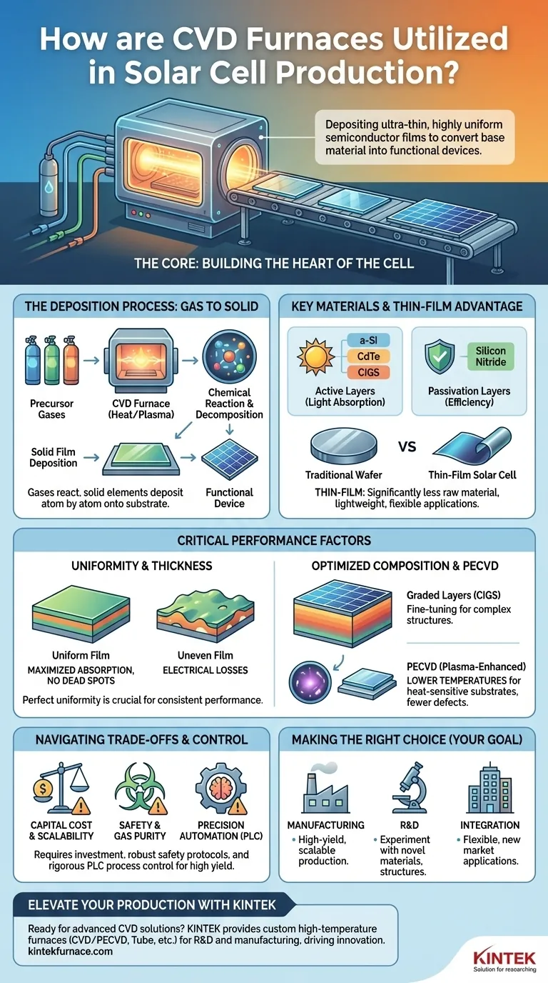
At its core, Chemical Vapor Deposition (CVD) furnaces are used in solar cell production to build the most critical component of the cell: the active photovoltaic layer. They do this by depositing an ultra-thin, highly uniform film of semiconductor material onto a substrate, converting a simple base material into a functional device that can turn light into electricity. This process is the foundation of modern thin-film solar cell manufacturing.
The true value of CVD in solar energy is not just that it deposits materials, but that it provides the atomic-level precision over film thickness and composition needed to maximize light absorption and electron flow. This control is what makes efficient, cost-effective thin-film solar cells a reality.
The Fundamental Role of CVD in Solar Cell Fabrication
To understand the importance of CVD furnaces, we must first understand the basic principle of the technology and how it constructs the heart of a solar cell.
From Gas to Solid: The Deposition Process
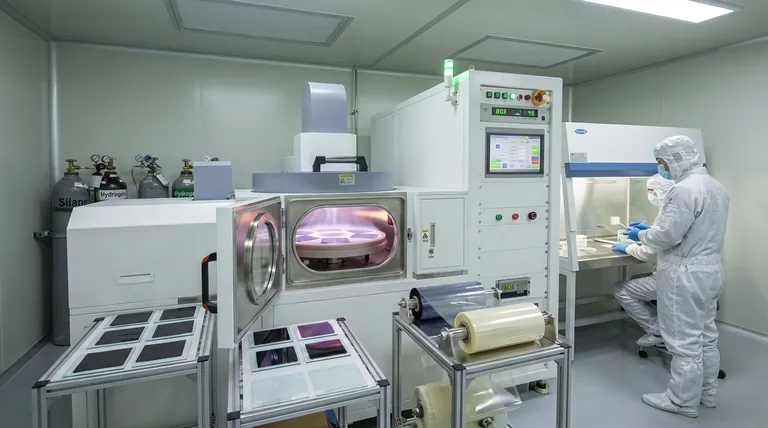
A CVD furnace is a high-temperature, vacuum-sealed chamber. Precursor gases containing the desired chemical elements are introduced into this chamber.
Inside, the high heat causes these gases to react and decompose. The solid elements from this reaction then "deposit" onto the surface of a substrate (like glass or flexible plastic), building a solid film one atomic layer at a time.
The Key Materials Deposited
CVD is used to create several essential layers in a thin-film solar cell, each with a specific function.
Common photovoltaic materials include amorphous silicon (a-Si), cadmium telluride (CdTe), and copper indium gallium selenide (CIGS). These are the "active" layers that absorb photons and generate charge carriers. Other materials like silicon nitride are deposited as anti-reflective or passivation layers to improve efficiency.
Why Thin-Film? The Manufacturing Advantage
Thin-film solar cells use significantly less raw material than traditional crystalline silicon wafers, making them potentially cheaper and more sustainable.
The CVD process is perfectly suited for this, creating films that are thousands of times thinner than a human hair. This enables the production of lightweight and even flexible solar panels, expanding their range of applications.
How CVD Directly Impacts Solar Cell Performance
The quality of the deposited film has a direct and profound impact on how well the final solar cell performs. CVD offers a level of control that is critical for maximizing this performance.
The Critical Factor: Film Thickness and Uniformity
For a solar cell to be efficient, the active layer must have a perfectly uniform thickness across the entire surface. Any variations or defects can create "dead spots" where light is not converted to electricity.
CVD excels at producing exceptionally uniform and homogenous films, ensuring consistent performance across the entire cell and minimizing electrical losses.
Optimizing Composition for Maximum Efficiency
Solar cell efficiency depends on the precise electronic properties of the semiconductor. CVD allows for fine-tuning the chemical composition of the film during deposition.
This enables the creation of complex structures, such as graded layers in CIGS cells where the material composition changes through the film's depth, optimizing the absorption of different wavelengths of light.
The Power of PECVD: Lower Temperatures, Higher Quality
A key variant is Plasma-Enhanced CVD (PECVD). This process uses an electrical field to generate plasma, which provides the energy for the chemical reaction instead of relying solely on high heat.
Depositing at lower temperatures is crucial for substrates that can't withstand high heat, like certain plastics. It also often results in higher-quality films with fewer defects, making PECVD a cornerstone of amorphous silicon solar cell manufacturing.
Understanding the Trade-offs and Process Control
While powerful, the CVD process is not without its challenges. It is a sophisticated industrial process that requires significant investment and expertise.
The Challenge of Scalability and Cost
CVD furnaces represent a significant capital expenditure. While they enable cost-effective materials usage, the initial investment in equipment and infrastructure is high.
Scaling the process for large-area deposition while maintaining perfect uniformity is a constant engineering challenge that directly impacts the final cost per watt of the solar panel.
Material Purity and Safety
The precursor gases used in CVD (such as silane for silicon deposition) can be highly toxic, flammable, or pyrophoric.
This necessitates complex and robust safety protocols, gas handling systems, and exhaust treatment, adding to the operational complexity and cost of a fabrication facility.
The Need for Precision Automation
The CVD process is extremely sensitive to variables like temperature, pressure, and gas flow rates. Even minor deviations can ruin the entire batch.
To ensure consistency and high yield, these furnaces are operated by a Programmable Logic Controller (PLC). This automation provides the rigorous process control necessary for repeatable, high-volume manufacturing.
Making the Right Choice for Your Goal
Understanding the role of CVD helps clarify its impact on different aspects of the solar industry. Your focus will determine which aspect of the technology is most relevant to you.
- If your primary focus is manufacturing efficiency: Recognize that CVD's ability to deposit uniform, large-area coatings is the key to high-yield, scalable production of thin-film panels.
- If your primary focus is research and development: Leverage CVD's versatility to experiment with novel material compositions, dopants, and multi-layer structures to push the boundaries of solar cell efficiency.
- If your primary focus is system integration: Appreciate that CVD enables lightweight and flexible thin-film cells, opening new markets and applications where traditional rigid panels are not viable.
Ultimately, CVD is the enabling technology that transforms raw gases into the high-performance heart of modern thin-film solar cells.
Summary Table:
| Aspect | Role in Solar Cell Production |
|---|---|
| Deposition Process | Converts precursor gases into solid films on substrates via high-temperature reactions. |
| Key Materials | Deposits amorphous silicon (a-Si), CdTe, CIGS, and silicon nitride for active and passivation layers. |
| Performance Impact | Ensures uniform thickness and composition for maximum light absorption and electron flow. |
| Technology Variants | Includes PECVD for lower-temperature deposition, ideal for heat-sensitive substrates. |
| Challenges | High capital cost, scalability issues, and safety requirements for toxic gases. |
Ready to elevate your solar cell production with advanced CVD solutions? Leveraging exceptional R&D and in-house manufacturing, KINTEK provides diverse laboratories with high-temperature furnace solutions like CVD/PECVD Systems, Muffle, Tube, Rotary, Vacuum & Atmosphere Furnaces. Our strong deep customization capability ensures precise alignment with your unique experimental needs, from enhancing efficiency in thin-film manufacturing to enabling flexible, cost-effective solar panels. Contact us today to discuss how our tailored furnace technologies can drive your innovations forward!
Visual Guide
Related Products
- Custom Made Versatile CVD Tube Furnace Chemical Vapor Deposition CVD Equipment Machine
- Split Chamber CVD Tube Furnace with Vacuum Station CVD Machine
- Multi Heating Zones CVD Tube Furnace Machine for Chemical Vapor Deposition Equipment
- Slide PECVD Tube Furnace with Liquid Gasifier PECVD Machine
- Controlled Inert Nitrogen Hydrogen Atmosphere Furnace
People Also Ask
- What is a CVD tube furnace and what is its primary function? Discover Precision Thin-Film Deposition
- What are the practical applications of gate media prepared by CVD tube furnaces? Unlock Advanced Electronics and More
- How can integrating CVD tube furnaces with other technologies benefit device fabrication? Unlock Advanced Hybrid Processes
- Why are CVD tube furnace sintering systems indispensable for 2D material research and production? Unlock Atomic-Scale Precision
- Which industries and research fields benefit from CVD tube furnace sintering systems for 2D materials? Unlock Next-Gen Tech Innovations


