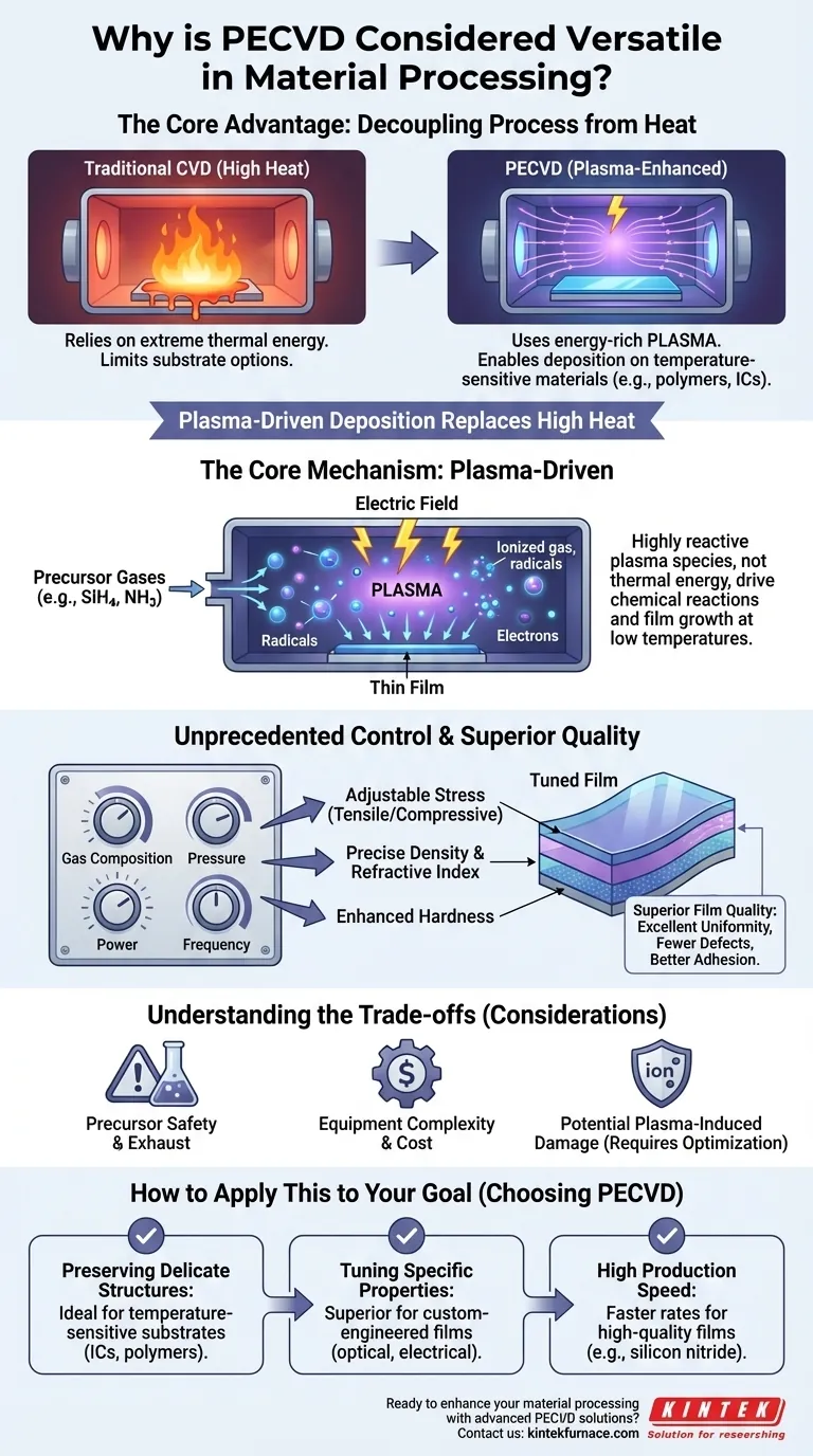
At its core, Plasma-Enhanced Chemical Vapor Deposition (PECVD) is exceptionally versatile because it decouples the deposition process from high temperatures. By using an energy-rich plasma rather than thermal energy to initiate chemical reactions, it can deposit a vast range of high-quality thin films onto nearly any type of material, including those that are temperature-sensitive. This fundamental capability unlocks applications that are impossible with traditional high-temperature methods.
The true versatility of PECVD lies not just in the variety of materials it can create, but in its ability to do so at low temperatures. This single advantage dramatically expands the universe of compatible substrates and preserves the integrity of delicate underlying structures.
The Core Mechanism: Plasma-Driven Deposition
The power of PECVD comes from how it generates the energy needed for film growth. Unlike conventional Chemical Vapor Deposition (CVD) which relies on high heat, PECVD uses an electromagnetic field to create plasma.
How Plasma Replaces High Heat
A PECVD process takes place in a low-pressure vacuum chamber. Precursor gases, such as silane (SiH4) and ammonia (NH3), are introduced into the chamber.
An electric field is then applied, which excites electrons and collides them with neutral gas molecules. This process creates plasma—an ionized gas containing a mix of ions, radicals, and electrons.
These highly reactive plasma species, not high temperatures, provide the energy needed to break chemical bonds and drive the reactions that form a thin film on the substrate's surface.
The Advantage of Low-Temperature Operation
The ability to generate reactive species without extreme heat is the single most important factor in PECVD's versatility.
This is critical in semiconductor manufacturing, as it allows for the deposition of high-quality insulating or conductive layers on top of complex, pre-existing circuits without causing thermal stress or damage.
It also enables coating on materials with low melting points, such as polymers and plastics, opening up applications in flexible electronics, optics, and medical devices.
Unprecedented Control Over Material Properties
The use of plasma provides a level of control that thermal processes cannot match. By adjusting the plasma parameters, engineers can precisely dictate the final properties of the deposited film.
Tuning the Plasma, Tuning the Film
Operators can independently adjust variables like gas composition, pressure, and the power and frequency of the electric field.
This direct control allows for the fine-tuning of critical film characteristics such as stress, density, refractive index, and hardness. You can engineer a film to be more compressive or tensile, more or less optically dense, or harder and more scratch-resistant.
Achieving Superior Film Quality
This precise control translates directly into higher-quality films. PECVD can produce layers with excellent uniformity across the entire substrate.
The resulting films are often denser, with fewer pinhole defects and better adhesion to the substrate compared to other methods. This leads to superior performance, including high chemical and thermal stability and excellent corrosion resistance.
Understanding the Trade-offs
While powerful, PECVD is not without its considerations. Its versatility comes with inherent complexities and limitations that must be managed.
Precursor Chemistry and Safety
PECVD can process solid, liquid, or gaseous precursors, but many of these chemicals can be hazardous, toxic, or pyrophoric (igniting on contact with air). Safe handling and exhaust management are critical operational requirements.
Equipment Complexity and Cost
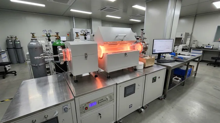
A PECVD system is a sophisticated piece of equipment involving a vacuum chamber, gas handling systems, and RF or microwave power supplies. This makes the initial capital investment and ongoing maintenance more significant than for some simpler deposition techniques.
Potential for Plasma-Induced Damage
The same energetic ions that enable low-temperature deposition can also, if not properly controlled, cause physical damage to the substrate surface through ion bombardment. Optimizing the process is a balancing act between achieving the desired film properties and minimizing this potential damage.
How to Apply This to Your Goal
Choosing a deposition method requires aligning the technique's strengths with your primary objective.
- If your primary focus is preserving delicate structures: PECVD is the definitive choice for depositing films on temperature-sensitive substrates like integrated circuits, polymers, or biological samples.
- If your primary focus is tuning specific film properties: The fine control over plasma parameters makes PECVD superior for creating materials with custom-engineered stress, optical, or electrical characteristics.
- If your primary focus is production speed for high-quality films: For materials like silicon nitride, PECVD offers significantly higher deposition rates than conventional CVD, improving throughput without sacrificing quality.
By leveraging plasma, PECVD provides an unparalleled combination of low-temperature processing and precise material control, making it a cornerstone technology for modern materials science.
Summary Table:
| Key Aspect | Benefit |
|---|---|
| Low-Temperature Operation | Enables deposition on temperature-sensitive materials like polymers and integrated circuits without damage |
| Precise Material Control | Allows tuning of film properties such as stress, density, and refractive index via plasma parameters |
| Wide Material Compatibility | Deposits high-quality thin films on nearly any substrate, expanding application possibilities |
| High Film Quality | Produces uniform, dense films with excellent adhesion and fewer defects for better performance |
Ready to enhance your material processing with advanced PECVD solutions? Leveraging exceptional R&D and in-house manufacturing, KINTEK provides diverse laboratories with tailored high-temperature furnace systems, including our versatile PECVD systems. Our strong deep customization capability ensures we precisely meet your unique experimental needs for low-temperature, high-quality thin film deposition. Contact us today to discuss how we can support your goals!
Visual Guide
Related Products
- RF PECVD System Radio Frequency Plasma Enhanced Chemical Vapor Deposition
- Slide PECVD Tube Furnace with Liquid Gasifier PECVD Machine
- Inclined Rotary Plasma Enhanced Chemical Deposition PECVD Tube Furnace Machine
- Inclined Rotary Plasma Enhanced Chemical Deposition PECVD Tube Furnace Machine
- Cylindrical Resonator MPCVD Machine System for Lab Diamond Growth
People Also Ask
- How does film quality compare between PECVD and CVD? Choose the Best Method for Your Substrate
- How is silicon dioxide deposited from tetraethylorthosilicate (TEOS) in PECVD? Achieve Low-Temperature, High-Quality SiO2 Films
- What are the key advantages of PECVD technology? Achieve Low-Temperature, High-Quality Thin Film Deposition
- What are the advantages of PECVD in film deposition? Achieve Low-Temp, High-Quality Coatings
- What are some promising applications of PECVD-prepared 2D materials? Unlock Advanced Sensing and Optoelectronics


