Knowledge Why is film uniformity important in semiconductor manufacturing? Ensure High Device Performance and Yield
Author avatar

Tech Team · Kintek Furnace

Updated 4 days ago

Why is film uniformity important in semiconductor manufacturing? Ensure High Device Performance and Yield


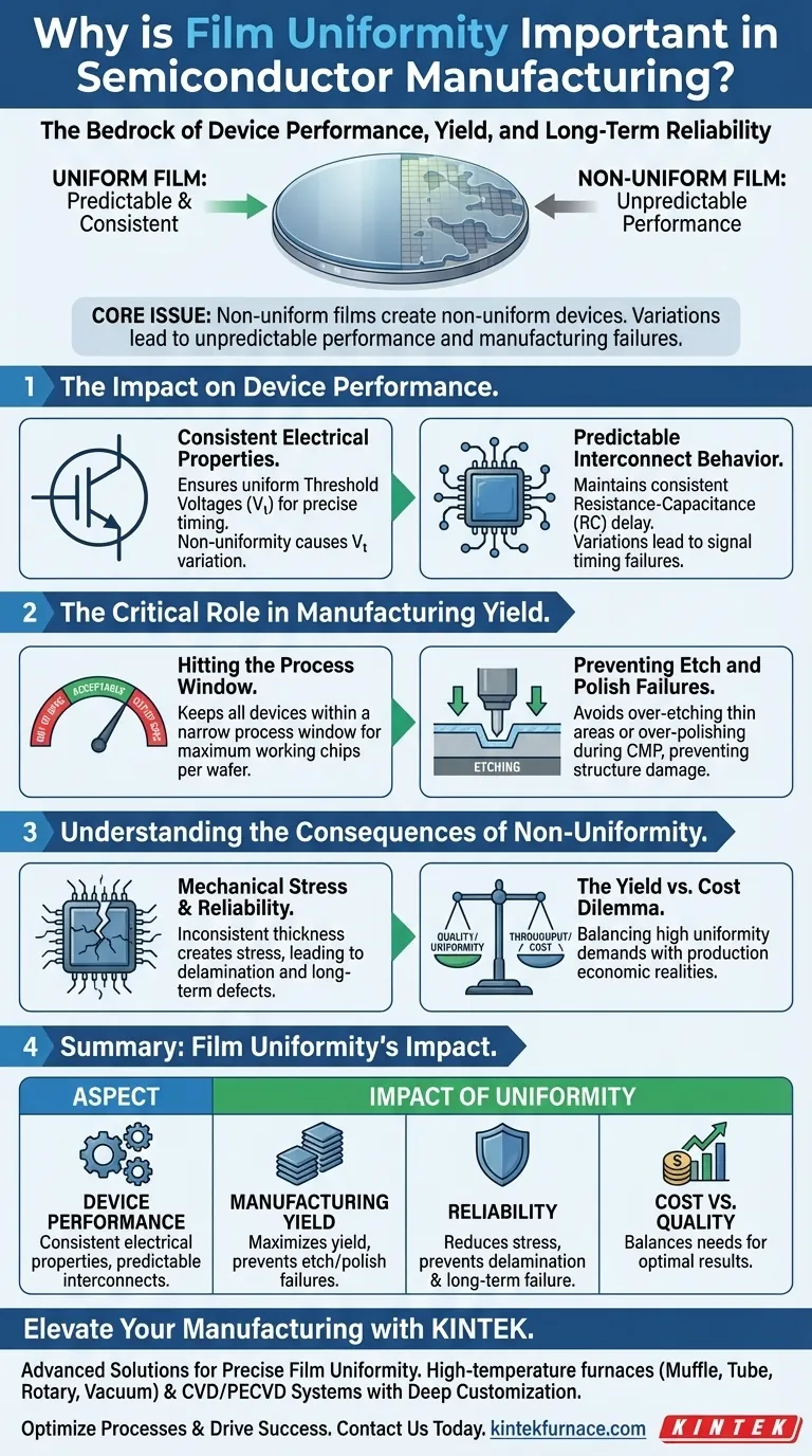
In semiconductor manufacturing, film uniformity is the bedrock of device performance, manufacturing yield, and long-term reliability. It is the critical factor that ensures every one of the billions of transistors on a silicon wafer behaves predictably and consistently. Without it, mass-producing functional integrated circuits would be impossible.

The core issue is simple: non-uniform films create non-uniform devices. When film thickness varies across a wafer, the electrical and physical properties of the transistors and interconnects also vary, leading to unpredictable performance and widespread manufacturing failures.

The Impact on Device Performance

At the nanometer scales of modern chips, even slight variations in film thickness have a dramatic effect on how the final device functions.

Consistent Electrical Properties

The thickness of a deposited film directly governs fundamental electrical characteristics. For example, the gate oxide layer in a transistor controls its switching behavior.

A non-uniform gate oxide means transistors in different locations will have different threshold voltages (Vt), causing them to turn on at different times. This variability destroys the precise timing required for a complex circuit to operate.

Predictable Interconnect Behavior

Similarly, the thickness of metal and dielectric layers determines the Resistance-Capacitance (RC) delay of the wires connecting transistors.

Variations in these films lead to inconsistent signal travel times across the chip. Some paths become too slow, causing timing failures that render the entire chip useless.

The Critical Role in Manufacturing Yield

Uniformity is not just about performance; it is a prerequisite for successfully manufacturing a device in the first place. Every step in the fabrication process is calibrated with the assumption of a uniform starting surface.

Hitting the Process Window

Semiconductor fabrication operates within an extremely narrow process window, which defines the acceptable range of parameters for a given step.

Excellent film uniformity ensures that all devices across the entire wafer fall within this critical window. Non-uniformity pushes devices "out of spec," directly causing a reduction in yield—the percentage of working chips per wafer.

Preventing Etch and Polish Failures

Subsequent manufacturing steps, like etching and Chemical-Mechanical Planarization (CMP), are highly dependent on film thickness.

If a film is not uniform, an etch process might completely remove the film in thinner areas before it has finished patterning the thicker areas. Likewise, CMP can over-polish thin regions, damaging underlying structures.

Understanding the Consequences of Non-Uniformity

Striving for uniformity is a constant battle against physical and chemical limitations. Failing to manage it has severe consequences.

Mechanical Stress and Reliability

When a film's thickness is inconsistent, it creates gradients in mechanical stress across the wafer.

These stress points can cause a number of long-term reliability failures, including film delamination (peeling), cracking, and other physical defects that emerge over the lifetime of the device.

The Yield vs. Cost Dilemma

Achieving near-perfect uniformity is technologically demanding and expensive. Deposition tools capable of higher uniformity often have lower throughput or higher costs.

Engineers must constantly balance the need for tighter uniformity against the economic realities of production. This trade-off between perfect quality and manufacturing cost is a central challenge in the industry.

Evaluating Uniformity for Your Goal

How you approach film uniformity depends on your specific role and objective.

  • If your primary focus is device design: You must incorporate expected film variations into your simulation models to ensure your chip is robust enough to function despite minor process imperfections.
  • If your primary focus is process integration: Your goal is to select and optimize deposition and etch processes to minimize within-wafer variation and maximize the process window for all manufacturing steps.
  • If your primary focus is reliability engineering: You must analyze how film non-uniformity creates stress points and use this data to predict and mitigate long-term failure modes.

Ultimately, controlling film uniformity is synonymous with controlling the performance, yield, and reliability of the final product.

Summary Table:

Aspect Impact of Film Uniformity
Device Performance Ensures consistent electrical properties and predictable interconnect behavior
Manufacturing Yield Keeps devices within process windows and prevents etch/polish failures
Reliability Reduces mechanical stress, preventing delamination and long-term failures
Cost vs. Quality Balances uniformity needs with production economics for optimal results

Elevate your semiconductor manufacturing with KINTEK's advanced solutions! Leveraging exceptional R&D and in-house manufacturing, we provide diverse laboratories with high-temperature furnace systems like Muffle, Tube, Rotary, Vacuum & Atmosphere Furnaces, and CVD/PECVD Systems. Our strong deep customization capability ensures precise film uniformity to meet your unique experimental requirements, boosting device performance, yield, and reliability. Contact us today to discuss how we can optimize your processes and drive success!

Visual Guide

Why is film uniformity important in semiconductor manufacturing? Ensure High Device Performance and Yield Visual Guide

Related Products

People Also Ask

Related Products

Multi Heating Zones CVD Tube Furnace Machine for Chemical Vapor Deposition Equipment

Multi Heating Zones CVD Tube Furnace Machine for Chemical Vapor Deposition Equipment

KINTEK's Multi-Zone CVD Tube Furnaces offer precision temperature control for advanced thin film deposition. Ideal for research and production, customizable for your lab needs.

Custom Made Versatile CVD Tube Furnace Chemical Vapor Deposition CVD Equipment Machine

Custom Made Versatile CVD Tube Furnace Chemical Vapor Deposition CVD Equipment Machine

KINTEK's CVD Tube Furnace offers precision temperature control up to 1600°C, ideal for thin film deposition. Customizable for research and industrial needs.

RF PECVD System Radio Frequency Plasma Enhanced Chemical Vapor Deposition

RF PECVD System Radio Frequency Plasma Enhanced Chemical Vapor Deposition

KINTEK RF PECVD System: Precision thin-film deposition for semiconductors, optics & MEMS. Automated, low-temperature process with superior film quality. Custom solutions available.

Slide PECVD Tube Furnace with Liquid Gasifier PECVD Machine

Slide PECVD Tube Furnace with Liquid Gasifier PECVD Machine

KINTEK Slide PECVD Tube Furnace: Precision thin film deposition with RF plasma, rapid thermal cycling, and customizable gas control. Ideal for semiconductors and solar cells.

HFCVD Machine System Equipment for Drawing Die Nano Diamond Coating

HFCVD Machine System Equipment for Drawing Die Nano Diamond Coating

KINTEK's HFCVD system delivers high-quality nano-diamond coatings for wire drawing dies, enhancing durability with superior hardness and wear resistance. Explore precision solutions now!

Split Chamber CVD Tube Furnace with Vacuum Station CVD Machine

Split Chamber CVD Tube Furnace with Vacuum Station CVD Machine

Split Chamber CVD Tube Furnace with Vacuum Station - High precision 1200°C lab furnace for advanced materials research. Customizable solutions available.

Inclined Rotary Plasma Enhanced Chemical Deposition PECVD Tube Furnace Machine

Inclined Rotary Plasma Enhanced Chemical Deposition PECVD Tube Furnace Machine

Advanced PECVD Tube Furnace for precise thin film deposition. Uniform heating, RF plasma source, customizable gas control. Ideal for semiconductor research.

1400℃ High Temperature Laboratory Tube Furnace with Quartz and Alumina Tube

1400℃ High Temperature Laboratory Tube Furnace with Quartz and Alumina Tube

KINTEK's Tube Furnace with Alumina Tube: Precision high-temperature processing up to 2000°C for labs. Ideal for material synthesis, CVD, and sintering. Customizable options available.

1700℃ High Temperature Laboratory Tube Furnace with Quartz or Alumina Tube

1700℃ High Temperature Laboratory Tube Furnace with Quartz or Alumina Tube

KINTEK's Tube Furnace with Alumina Tube: Precision heating up to 1700°C for material synthesis, CVD, and sintering. Compact, customizable, and vacuum-ready. Explore now!

Vertical Laboratory Quartz Tube Furnace Tubular Furnace

Vertical Laboratory Quartz Tube Furnace Tubular Furnace

Precision KINTEK Vertical Tube Furnace: 1800℃ heating, PID control, customizable for labs. Ideal for CVD, crystal growth & materials testing.

Molybdenum Vacuum Heat Treat Furnace

Molybdenum Vacuum Heat Treat Furnace

High-performance molybdenum vacuum furnace for precise 1400°C heat treatment. Ideal for sintering, brazing, and crystal growth. Durable, efficient, and customizable.

Electric Rotary Kiln Pyrolysis Furnace Plant Machine Small Rotary Kiln Calciner

Electric Rotary Kiln Pyrolysis Furnace Plant Machine Small Rotary Kiln Calciner

KINTEK Electric Rotary Kiln: Precise 1100℃ calcination, pyrolysis & drying. Eco-friendly, multi-zone heating, customizable for lab & industrial needs.

1700℃ High Temperature Muffle Oven Furnace for Laboratory

1700℃ High Temperature Muffle Oven Furnace for Laboratory

KT-17M Muffle Furnace: High-precision 1700°C lab furnace with PID control, energy efficiency, and customizable sizes for industrial & research applications.

Dental Porcelain Zirconia Sintering Ceramic Vacuum Press Furnace

Dental Porcelain Zirconia Sintering Ceramic Vacuum Press Furnace

Precision Vacuum Press Furnace for labs: ±1°C accuracy, 1200°C max, customizable solutions. Boost research efficiency today!

Laboratory Muffle Oven Furnace with Bottom Lifting

Laboratory Muffle Oven Furnace with Bottom Lifting

Boost lab efficiency with KT-BL Bottom Lifting Furnace: precise 1600℃ control, superior uniformity, and enhanced productivity for material science and R&D.

Vacuum Heat Treat Furnace with Ceramic Fiber Liner

Vacuum Heat Treat Furnace with Ceramic Fiber Liner

KINTEK's Vacuum Furnace with Ceramic Fiber Lining offers precise high-temperature processing up to 1700°C, ensuring uniform heat distribution and energy efficiency. Ideal for labs and production.

Small Vacuum Heat Treat and Tungsten Wire Sintering Furnace

Small Vacuum Heat Treat and Tungsten Wire Sintering Furnace

Compact vacuum tungsten wire sintering furnace for labs. Precise, mobile design with superior vacuum integrity. Ideal for advanced material research. Contact us!

Vacuum Heat Treat Sintering Furnace with Pressure for Vacuum Sintering

Vacuum Heat Treat Sintering Furnace with Pressure for Vacuum Sintering

KINTEK's Vacuum Pressure Sintering Furnace offers 2100℃ precision for ceramics, metals, and composites. Customizable, high-performance, and contamination-free. Get a quote now!

High Temperature Muffle Oven Furnace for Laboratory Debinding and Pre Sintering

High Temperature Muffle Oven Furnace for Laboratory Debinding and Pre Sintering

KT-MD Debinding & Pre-Sintering Furnace for ceramics - precise temperature control, energy-efficient design, customizable sizes. Boost your lab efficiency today!

1200℃ Controlled Inert Nitrogen Atmosphere Furnace

1200℃ Controlled Inert Nitrogen Atmosphere Furnace

KINTEK 1200℃ Controlled Atmosphere Furnace: Precision heating with gas control for labs. Ideal for sintering, annealing, and material research. Customizable sizes available.


Leave Your Message