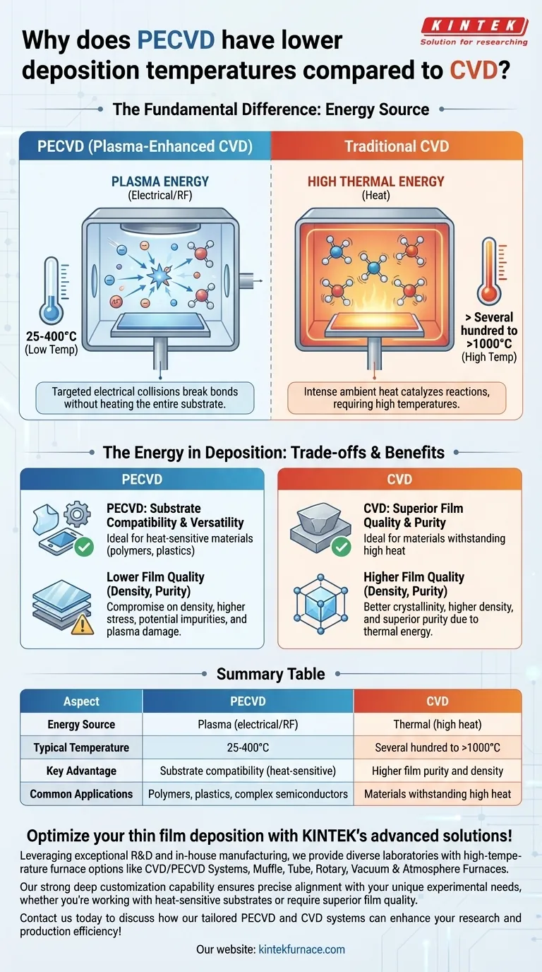
The fundamental difference is where the energy comes from. Plasma-Enhanced Chemical Vapor Deposition (PECVD) uses the electrical energy of a plasma to break down precursor gases, while conventional Chemical Vapor Deposition (CVD) relies exclusively on high thermal energy (heat) to achieve the same result. This allows PECVD to operate at significantly lower temperatures.
PECVD replaces the brute force of high heat with the targeted energy of a plasma. By using high-energy electrons and ions to initiate chemical reactions, it circumvents the need to heat the entire substrate to extreme temperatures, making it a fundamentally more versatile process for heat-sensitive materials.
The Role of Energy in Deposition
Every chemical vapor deposition process has one core requirement: providing enough energy to break down stable precursor gases into reactive species that can then form a solid thin film on a substrate. How that energy is delivered is what separates different CVD techniques.
How Traditional CVD Pays the Energy Bill
Traditional CVD operates on a simple principle: heat is the catalyst. The entire chamber, including the substrate, is heated to very high temperatures, often from several hundred to over a thousand degrees Celsius.
This intense thermal energy causes the precursor gas molecules to vibrate violently, eventually breaking their chemical bonds. These newly freed, reactive atoms then settle on the hot substrate surface to form the desired film.
How PECVD Finds an Alternative Energy Source
PECVD introduces a third element into the chamber: plasma. A plasma is an ionized gas created by applying a strong electric or radio-frequency (RF) field.
This plasma is a high-energy soup of ions, free radicals, and—most importantly—high-energy electrons. It is not necessarily "hot" in the traditional sense, but it is extremely reactive.
The Plasma Advantage: Energy Without Extreme Heat
In a PECVD system, collisions are the key. The high-energy electrons from the plasma collide with the precursor gas molecules.
These collisions transfer enough energy to break the molecular bonds, creating the same reactive species that high heat creates in traditional CVD. Because the energy for the reaction comes from these targeted electrical collisions rather than ambient heat, the substrate itself can remain at a much lower temperature, typically from room temperature to around 300-400°C.
Understanding the Trade-offs
The choice between PECVD and traditional CVD is not just about temperature; it's a decision based on balancing film quality, substrate limitations, and process complexity.
The Primary Benefit: Substrate Compatibility
The most significant advantage of PECVD's low-temperature process is its ability to deposit films on temperature-sensitive materials.
This includes polymers, plastics, and complex semiconductor devices with pre-existing metallic layers that would be damaged or melt at the high temperatures required for traditional CVD.
The Inherent Compromise: Film Quality
The lower deposition temperature of PECVD is also its primary source of compromise. Films deposited via PECVD often have different properties than those from high-temperature CVD.
They can have lower density, higher internal stress, and may incorporate impurities like hydrogen from the precursor gases. High-temperature CVD processes typically yield films with higher purity, better crystallinity, and superior density because the thermal energy helps atoms arrange into a more ideal structure.
Plasma-Induced Damage
While plasma enables the reaction, it can also cause damage. The bombardment of the substrate surface by energetic ions can create defects, which may be undesirable for highly sensitive electronic or optical applications.
Making the Right Choice for Your Goal
Selecting the correct deposition method requires a clear understanding of your project's primary objective.
- If your primary focus is depositing a film on a temperature-sensitive substrate: PECVD is the clear and often only viable choice.
- If your primary focus is achieving the highest possible film purity, density, and structural quality: High-temperature CVD is generally the superior method, assuming your substrate can withstand the heat.
Ultimately, the decision rests on balancing your material's thermal budget against the required performance characteristics of the final film.
Summary Table:
| Aspect | PECVD | CVD |
|---|---|---|
| Energy Source | Plasma (electrical/RF) | Thermal (high heat) |
| Typical Temperature | 25-400°C | Several hundred to >1000°C |
| Key Advantage | Substrate compatibility with heat-sensitive materials | Higher film purity and density |
| Common Applications | Polymers, plastics, complex semiconductors | Materials that can withstand high heat |
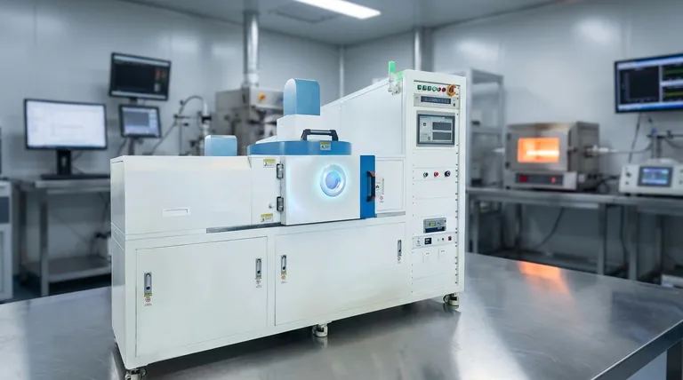
Optimize your thin film deposition with KINTEK's advanced solutions! Leveraging exceptional R&D and in-house manufacturing, we provide diverse laboratories with high-temperature furnace options like CVD/PECVD Systems, Muffle, Tube, Rotary, Vacuum & Atmosphere Furnaces. Our strong deep customization capability ensures precise alignment with your unique experimental needs, whether you're working with heat-sensitive substrates or require superior film quality. Contact us today to discuss how our tailored PECVD and CVD systems can enhance your research and production efficiency!
Visual Guide
Related Products
- Slide PECVD Tube Furnace with Liquid Gasifier PECVD Machine
- RF PECVD System Radio Frequency Plasma Enhanced Chemical Vapor Deposition
- Inclined Rotary Plasma Enhanced Chemical Deposition PECVD Tube Furnace Machine
- Inclined Rotary Plasma Enhanced Chemical Deposition PECVD Tube Furnace Machine
- Multi Heating Zones CVD Tube Furnace Machine for Chemical Vapor Deposition Equipment
People Also Ask
- What role does a Tube Furnace play in the CVD growth of carbon nanotubes? Achieve High-Purity CNT Synthesis
- What is plasma in the context of PECVD? Unlock Low-Temperature Thin Film Deposition
- How does PECVD equipment contribute to TOPCon bottom cells? Mastering Hydrogenation for Maximum Solar Efficiency
- What are the typical conditions for plasma-enhanced CVD processes? Achieve Low-Temperature Thin Film Deposition
- What are the disadvantages of tube furnace cracking when processing heavy raw materials? Avoid Costly Downtime and Inefficiency


