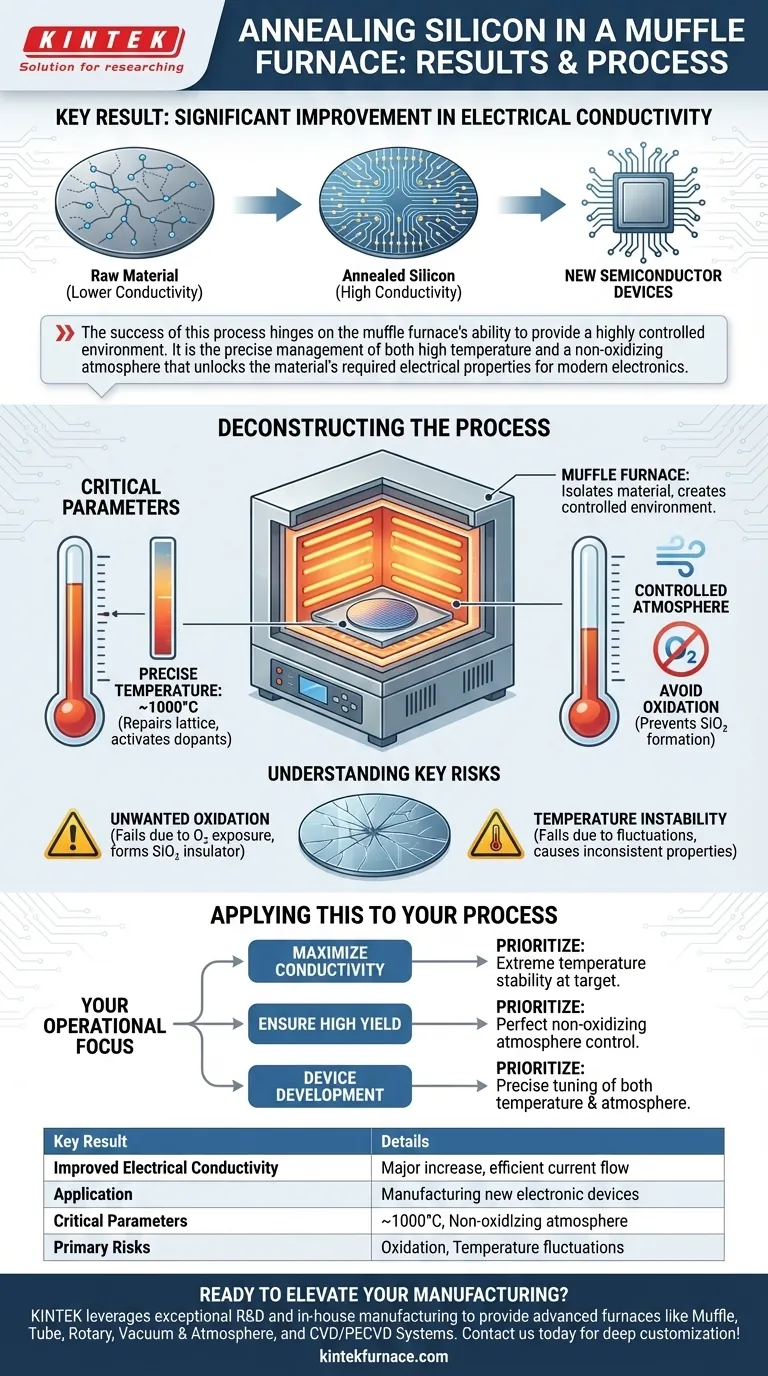
In short, annealing silicon-based materials in a muffle furnace resulted in a significant improvement in electrical conductivity. This enhancement was so effective that the material met the rigorous demands for electronic component production and was successfully used to manufacture new semiconductor devices.
The success of this process hinges on the muffle furnace's ability to provide a highly controlled environment. It is the precise management of both high temperature and a non-oxidizing atmosphere that unlocks the material's required electrical properties for modern electronics.
The Core Objective: Enhancing Electrical Properties
The entire purpose of annealing silicon is to fundamentally alter its physical structure to improve its performance in an electronic circuit. The process is a critical step in turning a raw material into a high-performance component.
The Immediate Outcome: A Significant Improvement
The most direct result observed after the heat treatment was a major increase in the material's electrical conductivity. This is the primary goal of annealing in this context, as it allows electrical current to flow more efficiently through the silicon.
The Practical Application: Enabling New Devices
This improved conductivity was not just a theoretical gain. It directly enabled the material to be used in the production of new semiconductor devices, validating the process as a viable and effective manufacturing step.
Deconstructing the Annealing Process
The results are a direct consequence of the specific conditions created within the muffle furnace. Understanding these parameters is key to replicating the success of the process.
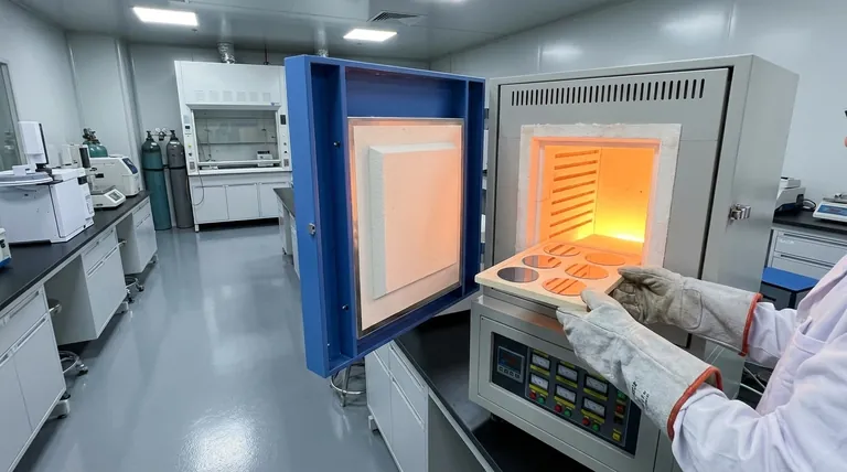
The Role of the Muffle Furnace
A muffle furnace was chosen because it isolates the material being heated from the fuel and combustion byproducts of the heat source. This creates an enclosed, controllable environment, which is essential for sensitive materials like silicon.
Critical Parameter 1: Precise Temperature
The process required a specific and stable high temperature. The furnace was controlled to maintain a temperature of approximately 1000°C. This level of thermal energy is necessary to repair defects in the silicon's crystal lattice and activate dopants within the material.
Critical Parameter 2: Controlled Atmosphere
Equally important was the control over the furnace's internal atmosphere. A key requirement was to avoid oxidation of the silicon. Exposing silicon to oxygen at high temperatures would create a layer of silicon dioxide (an insulator), destroying its semiconductor properties.
Understanding the Key Risks
While effective, this process is not without its challenges. The precision of the setup is what separates a successful outcome from a failed batch of materials.
The Primary Risk: Unwanted Oxidation
If the protective atmosphere inside the furnace fails, oxygen will react with the hot silicon. This forms a layer of silicon dioxide, which is essentially glass. An oxidized wafer is an electrical insulator, rendering it useless for semiconductor applications.
The Need for Stability
The target temperature of 1000°C is not a casual guideline. Temperature fluctuations during the process can lead to incomplete annealing or the introduction of thermal stress, resulting in inconsistent electrical properties across the material and poor device performance.
How to Apply This to Your Process
Your operational focus will determine which parameter you need to prioritize to achieve consistent, high-quality results.
- If your primary focus is maximizing conductivity: Your priority is achieving and holding the target annealing temperature with extreme stability.
- If your primary focus is ensuring high yield: You must perfect your atmosphere control to guarantee a non-oxidizing environment for every run.
- If your primary focus is device development: Treat annealing as a critical tuning step, where precise control over both temperature and atmosphere allows you to dial in the exact material properties your new device requires.
Ultimately, mastering the thermal treatment of silicon is fundamental to creating the high-performance electronic components that power our world.
Summary Table:
| Key Result | Details |
|---|---|
| Improved Electrical Conductivity | Major increase allowing efficient current flow in silicon materials |
| Application in Semiconductor Production | Enabled use in manufacturing new electronic devices |
| Critical Parameters | Temperature: ~1000°C, Non-oxidizing atmosphere to prevent SiO₂ formation |
| Primary Risks | Oxidation leading to insulation, temperature fluctuations causing inconsistencies |
Ready to elevate your semiconductor manufacturing with precise high-temperature solutions? KINTEK leverages exceptional R&D and in-house manufacturing to provide advanced furnaces like Muffle, Tube, Rotary, Vacuum & Atmosphere, and CVD/PECVD Systems. Our deep customization capabilities ensure your unique experimental needs are met for superior material properties. Contact us today to discuss how we can enhance your lab's efficiency and yield!
Visual Guide
Related Products
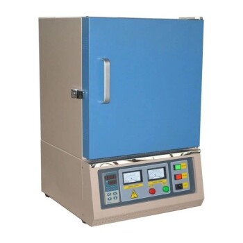
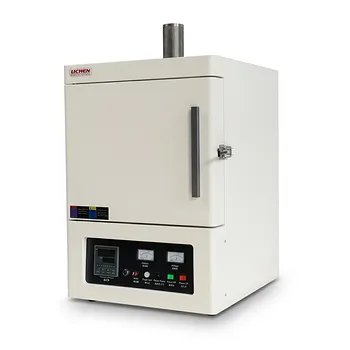
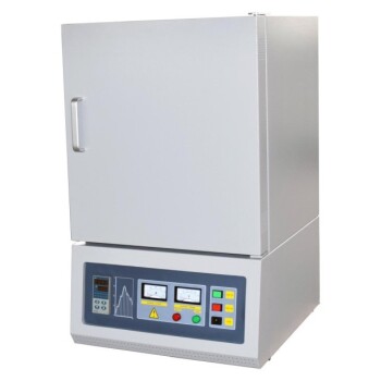
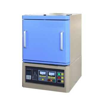
- 1400℃ Muffle Oven Furnace for Laboratory
- Laboratory Muffle Oven Furnace with Bottom Lifting
- High Temperature Muffle Oven Furnace for Laboratory Debinding and Pre Sintering
- 1200℃ Muffle Oven Furnace for Laboratory
- 1700℃ High Temperature Muffle Oven Furnace for Laboratory
People Also Ask
- What role does a muffle furnace play in refractory bricks? Enhance Performance and Durability Testing
- How is a laboratory high-temperature muffle furnace utilized to achieve the specific crystalline structure of LaFeO3 catalysts?
- What function does a muffle furnace perform in perovskite formation? Optimize Your Thermal Synthesis
- Function of Muffle Furnace in Exfoliating g-C3N4 Nanosheets: Precision Thermal Control and Defect Engineering
- How does a high-temperature laboratory muffle furnace affect material properties? Transform Anodic Oxide Films Fast