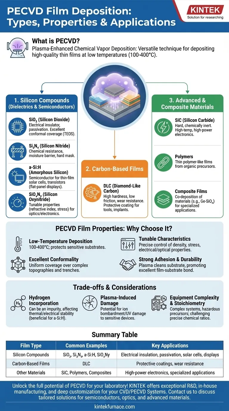
In short, Plasma-Enhanced Chemical Vapor Deposition (PECVD) is a highly versatile technique capable of depositing a wide range of thin films. The most common materials include silicon-based compounds like silicon oxide (SiO₂) and silicon nitride (Si₃N₄), carbon-based films like diamond-like carbon (DLC), and semiconductors such as amorphous silicon (a-Si:H). This versatility makes PECVD a cornerstone technology in semiconductor manufacturing, optics, and materials science.
The true value of PECVD is not just the variety of materials it can deposit, but its ability to create high-quality, customized films at low temperatures. This allows for the engineering of specific properties on substrates that could not survive traditional high-temperature deposition methods.
The Core Film Categories of PECVD
PECVD's flexibility stems from its use of plasma to energize precursor gases, allowing film deposition to occur at significantly lower temperatures than conventional Chemical Vapor Deposition (CVD). This opens the door to a diverse materials palette.
Silicon Compounds (Dielectrics and Semiconductors)
This is the most common and critical category for PECVD. These films are the building blocks of modern microelectronics.
- Silicon Dioxide (SiO₂): Used extensively as an electrical insulator and a passivation layer to protect device surfaces. PECVD can produce high-quality SiO₂, including films from TEOS precursors that offer excellent, void-free coverage over complex surface topographies.
- Silicon Nitride (Si₃N₄): Valued for its high chemical resistance and effectiveness as a moisture and ion barrier. It serves as a durable passivation layer and a hard mask in fabrication processes.
- Amorphous Silicon (a-Si:H): A key semiconductor material used in thin-film solar cells and transistors for large-area electronics like flat-panel displays. The hydrogen incorporation during PECVD is critical for its electronic properties.
- Silicon Oxynitride (SiOxNy): By controlling the gas mixture, the properties of the film can be tuned between those of an oxide and a nitride, allowing for precise control over refractive index and stress for optical and electronic applications.
Carbon-Based Films
PECVD is also a leading method for producing hard, durable carbon films.
- Diamond-Like Carbon (DLC): This is not pure diamond but an amorphous carbon film with a high degree of hardness, low friction, and excellent wear resistance. It is widely used as a protective coating for mechanical parts, medical implants, and cutting tools.
Other Advanced and Composite Materials
The capability of PECVD extends beyond the standard silicon and carbon families.
- Silicon Carbide (SiC): A hard, chemically inert material used in high-temperature, high-power electronics and as a protective coating.
- Polymers: PECVD can polymerize certain organic precursor gases to create thin, polymer-like films with unique chemical and electrical properties.
- Composite Films: The process allows for the co-deposition of different materials, creating composites like Germanium-Silicon-Oxide (Ge-SiOx) or even certain metal films for specialized applications.
Why Choose PECVD? The Resulting Film Properties
The decision to use PECVD is often driven by the unique properties the resulting films exhibit, which are a direct consequence of the low-temperature, plasma-driven process.
High-Quality Films at Lower Temperatures
This is the primary advantage of PECVD. Deposition can occur at temperatures from 100-400°C, compared to 600-900°C for many conventional CVD methods. This prevents damage to sensitive substrates, such as plastics, or previously fabricated layers on a silicon wafer.
Excellent Conformality and Coverage
PECVD excels at depositing films that uniformly coat complex, three-dimensional structures. This "conformal coverage" is essential in microfabrication, where films must evenly cover the vertical sidewalls and horizontal surfaces of microscopic trenches and features without creating voids.
Tunable Film Characteristics
By precisely controlling process parameters like gas flow rates, pressure, power, and temperature, operators can fine-tune the film's properties. This allows for the customization of a film's density, stress, chemical resistance, electrical behavior, or optical transparency for a specific application.
Strong Adhesion and Durability
The plasma environment often cleans and activates the substrate surface just before deposition, promoting excellent adhesion between the film and the substrate. The resulting films are typically dense, uniform, and resistant to cracking, leading to more reliable and durable devices.
Understanding the Trade-offs
While powerful, PECVD is not without its complexities and limitations. An objective assessment requires acknowledging these trade-offs.
Hydrogen Incorporation
Because hydrogen-containing precursors (like silane, SiH₄) are common, PECVD films often contain a significant amount of hydrogen. While beneficial for amorphous silicon, this can be an undesirable impurity in other films, potentially affecting thermal stability and electrical properties.
Plasma-Induced Damage
The same plasma that enables low-temperature deposition can also cause damage to the substrate or the growing film if not carefully controlled. This can include ion bombardment or UV radiation effects, which may impact the performance of sensitive electronic devices.
Film Stoichiometry Control
Achieving the exact chemical ratio (stoichiometry)—for instance, a perfect Si₃N₄—can be more challenging in PECVD than in high-temperature methods. PECVD nitride is often written as SiNx, acknowledging that it is not perfectly stoichiometric, which can alter its properties.
Precursor and Equipment Complexity
PECVD systems are complex machines, and the precursor gases used can be hazardous, pyrophoric, or toxic, requiring stringent safety protocols. This adds to the operational cost and complexity compared to simpler methods like PVD.
Making the Right Choice for Your Application
Selecting a deposition method depends entirely on your end goal. PECVD offers a unique combination of versatility, quality, and low-temperature processing.
- If your primary focus is electrical insulation and passivation on a finished device: PECVD-deposited Silicon Nitride or Silicon Dioxide is the industry standard due to its quality and low-temperature budget.
- If your primary focus is mechanical hardness and wear resistance: Diamond-Like Carbon (DLC) is an excellent choice for creating durable, low-friction surfaces.
- If your primary focus is thin-film solar cells or large-area displays: PECVD is the essential technology for depositing the active Amorphous Silicon (a-Si:H) layers.
- If your primary focus is coating complex 3D microstructures uniformly: TEOS-based PECVD for Silicon Dioxide provides superior conformal coverage compared to many other techniques.
Ultimately, PECVD empowers engineers and scientists to engineer materials at the atomic level, making it an indispensable tool for creating next-generation technology.
Summary Table:
| Film Type | Common Examples | Key Applications |
|---|---|---|
| Silicon Compounds | SiO₂, Si₃N₄, a-Si:H, SiOxNy | Electrical insulation, passivation, solar cells, displays |
| Carbon-Based Films | Diamond-Like Carbon (DLC) | Protective coatings, wear resistance |
| Other Materials | SiC, Polymers, Composites | High-power electronics, specialized applications |
Unlock the full potential of PECVD for your laboratory! At KINTEK, we leverage exceptional R&D and in-house manufacturing to provide advanced high-temperature furnace solutions, including CVD/PECVD Systems. Our strong deep customization capability ensures we can precisely meet your unique experimental requirements, whether you're working with semiconductors, optics, or advanced materials. Contact us today to discuss how our tailored PECVD solutions can enhance your research and development outcomes!
Visual Guide
Related Products
- Slide PECVD Tube Furnace with Liquid Gasifier PECVD Machine
- RF PECVD System Radio Frequency Plasma Enhanced Chemical Vapor Deposition
- Inclined Rotary Plasma Enhanced Chemical Deposition PECVD Tube Furnace Machine
- Inclined Rotary Plasma Enhanced Chemical Deposition PECVD Tube Furnace Machine
- Multi Heating Zones CVD Tube Furnace Machine for Chemical Vapor Deposition Equipment
People Also Ask
- In which industries is the tube furnace commonly used? Essential for Materials Science, Energy, and More
- What are the disadvantages of tube furnace cracking when processing heavy raw materials? Avoid Costly Downtime and Inefficiency
- What is plasma in the context of PECVD? Unlock Low-Temperature Thin Film Deposition
- How does PECVD equipment contribute to TOPCon bottom cells? Mastering Hydrogenation for Maximum Solar Efficiency
- What are the main advantages of PECVD tube furnaces compared to CVD tube furnaces? Lower Temp, Faster Deposition, and More


