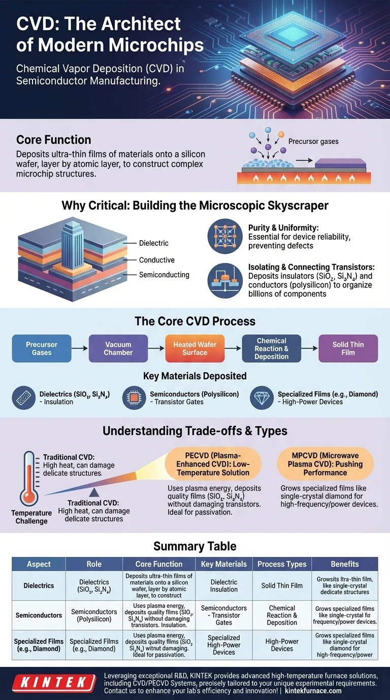
At its core, Chemical Vapor Deposition (CVD) is the architectural process used to construct the intricate, multi-layered structures of modern microchips. It functions by depositing exceptionally thin films of various materials onto a silicon wafer, layer by atomic layer. This precise deposition is what allows for the creation of insulating, conductive, and semiconducting components that form the foundation of all integrated circuits.
The true role of CVD is not merely to add layers to a chip, but to enable the extreme complexity of modern electronics. Its ability to deposit pristine, uniform films with atomic-scale control is the fundamental capability that allows billions of transistors to be built and function reliably on a tiny piece of silicon.
Why Thin Film Deposition is Critical
The function of a semiconductor device is defined by the precise arrangement of different materials. CVD is the primary method for building this arrangement vertically.
Building the Skyscraper of a Microchip
An integrated circuit is not a flat, two-dimensional object. It is a microscopic skyscraper, with dozens or even hundreds of layers of different materials stacked on top of one another.
CVD is the technique used to "pour the concrete" and "install the wiring" for each floor of this skyscraper, forming the dielectric (insulating) and conductive layers that make the chip work.
The Need for Purity and Uniformity
Every layer deposited must be almost perfectly uniform and free of defects. Even a single misplaced atom or microscopic impurity can cause a short circuit or a device failure.
The reliability and performance of an advanced semiconductor depend directly on the quality of these deposited films. CVD is valued for its ability to produce highly uniform, defect-free layers across an entire wafer.
Isolating and Connecting Transistors
Modern chips contain billions of transistors in a very small space. To prevent electrical chaos, these components must be perfectly insulated from one another.
CVD is used to deposit dielectric films like silicon dioxide (SiO₂) and silicon nitride (Si₃N₄), which act as insulators. It also deposits conductive films like polysilicon that form the gates of transistors or the "wires" connecting them.
The Core CVD Process
CVD is a highly controlled chemical process that turns gases into solid films.
How it Works in Principle
Imagine steam condensing on a cold mirror. CVD operates on a similar principle but involves a chemical reaction.
Precursor gases containing the atoms you want to deposit (e.g., silicon) are introduced into a vacuum chamber. When these gases come into contact with the heated surface of the silicon wafer, they react and deposit a solid, thin film of the desired material.
Key Materials Deposited by CVD
CVD is versatile and can deposit the most critical materials in chip fabrication, including:
- Dielectrics: Silicon dioxide (SiO₂) and silicon nitride (Si₃N₄) for insulation.
- Semiconductors: Polysilicon, a foundational material for building transistor gates.
- Specialized Films: Advanced materials like single-crystal diamond for high-power devices.
Understanding the Trade-offs
Not all CVD processes are the same. The choice of method depends on the specific requirements of the fabrication step, with temperature being a primary constraint.
The Temperature Challenge
Traditional CVD methods require very high temperatures to trigger the chemical reaction on the wafer's surface.
While effective, this high heat can damage or alter the delicate structures that have already been built in previous steps. This is a significant problem in complex, multi-layered chip designs.
PECVD: The Low-Temperature Solution
Plasma-Enhanced CVD (PECVD) is a critical innovation that solves the temperature problem. It uses an electromagnetic field (plasma) to energize the precursor gases, allowing the deposition reaction to occur at much lower temperatures.
This low-temperature processing is essential for modern manufacturing, enabling the deposition of high-quality insulating films like SiO₂ and Si₃N₄ without damaging the underlying transistors. It is also used for surface passivation, which protects the finished device.
MPCVD: Pushing Performance Boundaries
For next-generation applications, even more specialized techniques are used. Microwave Plasma CVD (MPCVD) is used to grow films with exceptional properties, like single-crystal diamond.
These diamond substrates offer superior thermal conductivity and electrical properties, enabling the creation of high-frequency and high-power electronic devices for advanced telecommunications and computing.
Making the Right Choice for Your Goal
The specific CVD technique is chosen based on the desired material properties and its position within the chip's complex architecture.
- If your primary focus is foundational logic and memory: Standard CVD and PECVD are the workhorses for depositing the core polysilicon, silicon dioxide, and silicon nitride layers.
- If your primary focus is protecting the device or insulating upper layers: PECVD is the ideal choice due to its low-temperature process, which prevents damage to the sensitive transistor structures below.
- If your primary focus is high-power or high-frequency electronics: Advanced methods like MPCVD are required to create specialized films like diamond that offer extreme performance characteristics.
Understanding the role of CVD is to understand that a microchip is meticulously grown, not just assembled.
Summary Table:
| Aspect | Role in Semiconductor Manufacturing |
|---|---|
| Core Function | Deposits thin films for insulating, conductive, and semiconducting layers on silicon wafers |
| Key Materials | Silicon dioxide (SiO₂), silicon nitride (Si₃N₄), polysilicon, and specialized films like diamond |
| Process Types | Standard CVD, Plasma-Enhanced CVD (PECVD), Microwave Plasma CVD (MPCVD) |
| Benefits | Enables high uniformity, defect-free layers, and supports complex, multi-layered chip architectures |
Leveraging exceptional R&D and in-house manufacturing, KINTEK provides diverse laboratories with advanced high-temperature furnace solutions. Our product line, including Muffle, Tube, Rotary Furnaces, Vacuum & Atmosphere Furnaces, and CVD/PECVD Systems, is complemented by our strong deep customization capability to precisely meet unique experimental requirements. If you're involved in semiconductor manufacturing and need reliable CVD equipment for precise thin film deposition, contact us today to enhance your lab's efficiency and innovation!
Visual Guide
Related Products
- Custom Made Versatile CVD Tube Furnace Chemical Vapor Deposition CVD Equipment Machine
- Multi Heating Zones CVD Tube Furnace Machine for Chemical Vapor Deposition Equipment
- HFCVD Machine System Equipment for Drawing Die Nano Diamond Coating
- Split Chamber CVD Tube Furnace with Vacuum Station CVD Machine
- 915MHz MPCVD Diamond Machine Microwave Plasma Chemical Vapor Deposition System Reactor
People Also Ask
- What are the benefits of developing new precursor materials for CVD tube furnaces? Unlock Advanced Thin-Film Synthesis
- What is the working principle of a CVD tube furnace? Achieve Precise Thin Film Deposition for Your Lab
- What are the practical applications of gate media prepared by CVD tube furnaces? Unlock Advanced Electronics and More
- What are the key application fields of CVD tube furnaces? Unlock Precision in Thin-Film Synthesis
- What is a CVD tube furnace and what is its primary function? Discover Precision Thin-Film Deposition


