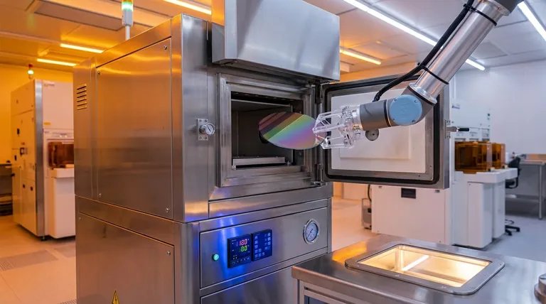
In short, inert atmosphere furnaces are indispensable in the semiconductor industry because they create an ultra-pure, oxygen-free environment. This is essential for high-temperature processes like annealing and dopant activation, where any reaction with oxygen would contaminate the silicon wafer, create defects, and ultimately render the microchip useless.
The core function of an inert atmosphere furnace is not just to provide heat, but to act as a protective shield. By replacing reactive air with a neutral gas like nitrogen or argon, it ensures that high-temperature manufacturing steps only alter the silicon wafer in precisely intended ways, guaranteeing the material purity and electrical integrity required for modern electronics.
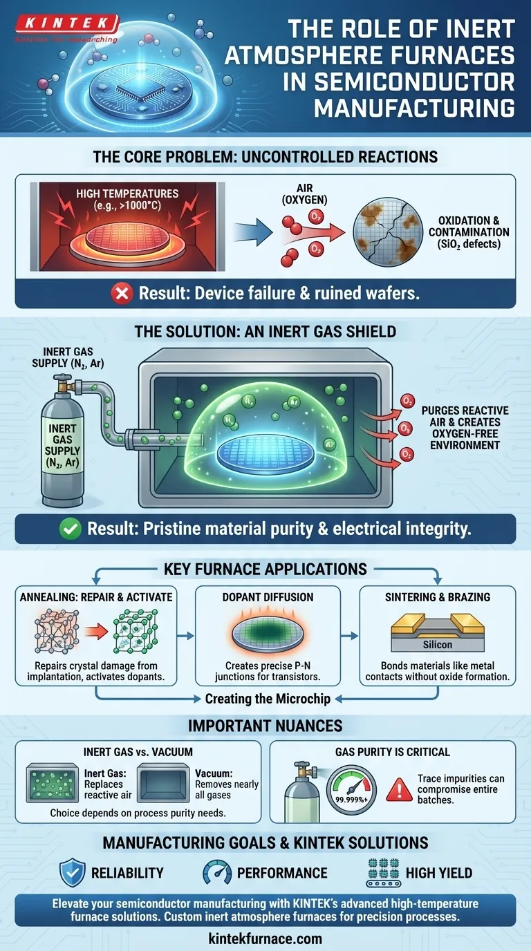
The Core Problem: Uncontrolled Reactions at High Temperatures
Semiconductor fabrication relies on extreme heat to modify the properties of silicon wafers. However, this same heat creates a significant vulnerability to contamination from the surrounding atmosphere.
The Double-Edged Sword of Heat
High temperature is necessary to perform critical steps like repairing crystal structures (annealing) or activating implanted dopant atoms. It gives atoms the energy they need to move into their correct positions within the silicon lattice.
However, this thermal energy also dramatically accelerates chemical reactions. At the temperatures used in fabrication (often exceeding 1000°C), a silicon wafer exposed to normal air would be instantly and catastrophically compromised.
The Primary Threat: Oxidation
The most significant threat is oxygen. When heated, silicon reacts readily with oxygen to form a layer of silicon dioxide (SiO₂).
While a controlled layer of SiO₂ is sometimes created intentionally for insulation, uncontrolled oxidation is disastrous. It creates defects, alters the carefully engineered electrical pathways, and prevents other processes from working correctly, leading to device failure.
The Solution: An Inert Gas Shield
An inert atmosphere furnace solves this problem by completely purging the processing chamber of ambient air and replacing it with an inert gas, most commonly nitrogen (N₂) or argon (Ar).
These gases are chemically non-reactive. They provide the necessary atmospheric pressure to facilitate stable heating but will not react with the silicon wafer, even at extreme temperatures. This creates a pristine environment where thermal processes can occur without unwanted chemical side effects.
Key Furnace Applications in Semiconductor Fabrication
By preventing oxidation and contamination, inert atmosphere furnaces enable several foundational steps in creating a microchip.
Annealing: Repairing and Activating
Processes like ion implantation, which embeds dopant atoms into the silicon, cause significant damage to the wafer's crystalline structure. Annealing is a controlled heating process that repairs this damage.
Simultaneously, annealing provides the energy needed to activate the dopants, allowing them to integrate into the silicon lattice and become electrically active. The inert atmosphere ensures this repair and activation happens cleanly.
Dopant Diffusion
Diffusion is the process of using heat to cause dopants to spread out from an area of high concentration to an area of low concentration. This is used to create the specific P-N junctions that form transistors.
Performing this at high temperatures in an inert environment ensures the dopants diffuse evenly and predictably, without reacting with oxygen.
Sintering and Brazing
These processes use heat to bond different materials together. For instance, sintering is used to densify metal contacts on the wafer.
An inert atmosphere is critical here to prevent oxides from forming on the metal surfaces, as oxides would create a weak, unreliable bond and increase electrical resistance.
Understanding the Nuances and Alternatives
While essential, inert gas furnaces are part of a broader family of controlled-environment tools. Understanding the differences is key.
Inert Gas vs. Vacuum
A vacuum furnace achieves a pure environment by removing nearly all gases, creating a near-vacuum. An inert gas furnace achieves it by replacing reactive gases with non-reactive ones.
The choice depends on the process. A vacuum is often used for the highest-purity applications where even the presence of argon is undesirable. Inert gas is more common for processes like annealing where the primary goal is simply to prevent oxidation at a lower cost than maintaining a hard vacuum.
The Importance of Gas Purity
The effectiveness of an inert atmosphere furnace is entirely dependent on the purity of the inert gas supply. Even trace amounts of oxygen or moisture in the nitrogen or argon can be enough to compromise an entire batch of wafers, making gas purification systems a critical part of the infrastructure.
Controlled Reactive Atmospheres
It's important to note that the same furnace technology can be used for processes that require a reactive gas. For example, the intentional growth of a silicon dioxide gate layer is done in a furnace filled with pure, controlled oxygen.
The underlying principle is atmospheric control. The furnace provides the platform to create any specific gaseous environment needed, whether it's perfectly inert or precisely reactive.
Making the Right Choice for Manufacturing Goals
The use of inert atmospheres is not a choice but a necessity, directly tied to the fundamental goals of semiconductor manufacturing.
- If your primary focus is reliability: An inert atmosphere is the first line of defense against microscopic defects and unwanted chemical layers that cause long-term component failure.
- If your primary focus is performance: Preventing contamination ensures the finished chip has the exact electrical properties designed for high-speed, low-power operation.
- If your primary focus is manufacturing yield: The repeatable, controlled environment provided by these furnaces is what allows for the mass production of millions of identical, functional chips from every wafer.
Ultimately, this precise control over the manufacturing environment is a foundational pillar that makes the digital world possible.
Summary Table:
| Application | Purpose | Benefit |
|---|---|---|
| Annealing | Repair crystal damage and activate dopants | Ensures clean, defect-free silicon wafers |
| Dopant Diffusion | Create P-N junctions for transistors | Allows even, predictable dopant spread |
| Sintering/Brazing | Bond materials like metal contacts | Prevents oxide formation for strong bonds |
Elevate your semiconductor manufacturing with KINTEK's advanced high-temperature furnace solutions! Leveraging exceptional R&D and in-house manufacturing, we provide inert atmosphere furnaces tailored for precise annealing, dopant activation, and more. Our product line includes Muffle, Tube, Rotary, Vacuum & Atmosphere Furnaces, and CVD/PECVD Systems, with deep customization to meet your unique experimental needs. Ensure purity, reliability, and high yield—contact us today to discuss how we can optimize your processes!
Visual Guide
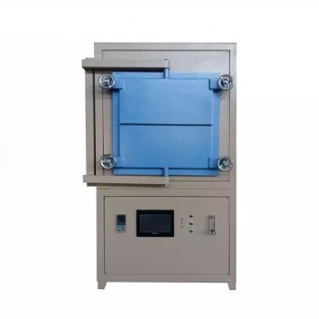
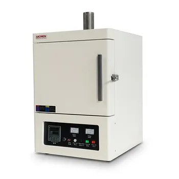
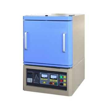
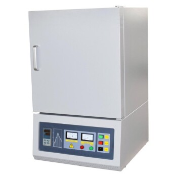
Related Products
- 1400℃ Controlled Inert Nitrogen Atmosphere Furnace
- 1700℃ Controlled Inert Nitrogen Atmosphere Furnace
- Controlled Inert Nitrogen Hydrogen Atmosphere Furnace
- 1200℃ Controlled Inert Nitrogen Atmosphere Furnace
- Mesh Belt Controlled Atmosphere Furnace Inert Nitrogen Atmosphere Furnace
People Also Ask
- How are inert atmosphere furnaces used in the ceramics industry? Ensure Purity and Performance in High-Temp Processing
- Which gases are commonly used to create inert atmospheres in furnaces? Nitrogen vs. Argon Explained
- What does inert mean in furnace atmospheres? Protect materials from oxidation with inert gases.
- What are the main purposes of using an inert atmosphere? Prevent Oxidation and Ensure Process Safety
- How are inert atmosphere furnaces sealed and prepared for operation? Ensure Process Integrity and Prevent Oxidation