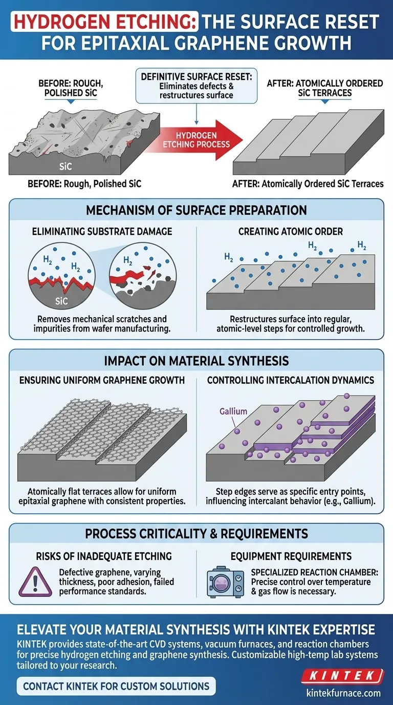
The significance of hydrogen etching lies in its ability to act as a definitive surface reset for Silicon Carbide (SiC) substrates prior to growth. This pre-treatment eliminates physical defects such as scratches and impurities while simultaneously restructuring the surface into regular, atomic-level steps to ensure high-quality material synthesis.
Core Takeaway Achieving a pristine starting surface is the single most critical factor for successful epitaxy. Hydrogen etching transforms a rough, polished substrate into an atomically ordered landscape, which is a prerequisite for growing uniform graphene and controlling the behavior of intercalated atoms like gallium.
The Mechanism of Surface Preparation
Eliminating Substrate Damage
Raw Silicon Carbide (SiC) substrates often arrive with microscopic imperfections.
Mechanical polishing processes used during wafer manufacturing leave behind surface scratches and impurities. Hydrogen etching in a reaction chamber effectively removes these layers, stripping away the damaged material to reveal the pristine crystal underneath.
Creating Atomic Order
Beyond simple cleaning, this process fundamentally restructures the surface morphology.
The etching creates regular, atomic-level steps across the substrate. This transition from a random, rough surface to an ordered, terraced structure is the physical foundation required for controlled epitaxial growth.
Impact on Material Synthesis
Ensuring Uniform Graphene Growth
The quality of epitaxial graphene is directly dependent on the quality of the underlying SiC surface.
Without the regular step structure provided by hydrogen etching, graphene growth would be disjointed and irregular. The atomically flat terraces allow the carbon atoms to arrange themselves into a uniform epitaxial graphene layer with consistent electronic properties.
Controlling Intercalation Dynamics
For advanced applications involving the insertion of other elements between layers, the surface structure is a control mechanism.
The primary reference notes that this process directly influences the intercalation dynamics of gallium atoms. The step edges created during etching serve as specific entry points or pathways, allowing for precise control over how foreign atoms interact with the graphene-substrate interface.
Understanding the Process Criticality
The Risks of Inadequate Etching
Skipping or shortening this pre-treatment step is a common point of failure.
If the surface retains scratches or lacks defined atomic steps, the subsequent graphene layer will likely suffer from defects, varying thickness, or poor adhesion. The result is a material that fails to meet electronic performance standards.
Equipment Requirements
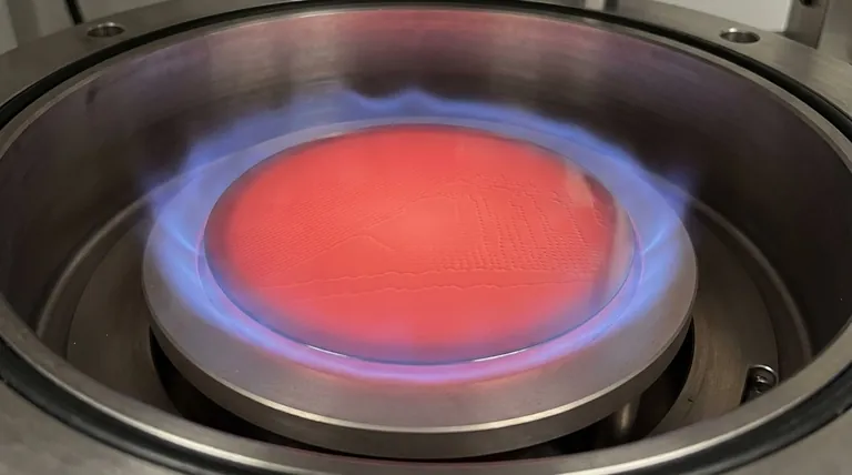
This process cannot be performed loosely; it requires a specialized reaction chamber.
Precise control over temperature and gas flow is necessary to etch the SiC without degrading the crystal quality. This highlights that hydrogen etching is not merely a cleaning wipe, but a sophisticated thermodynamic process.
Making the Right Choice for Your Goal
When planning your epitaxial growth recipe, consider how hydrogen etching aligns with your specific targets:
- If your primary focus is Material Uniformity: Ensure the etching duration is sufficient to fully remove polishing damage and establish clear atomic terraces.
- If your primary focus is Intercalation (e.g., Gallium): Optimize the step morphology during etching, as the step edges will define how effectively the intercalant penetrates the interface.
Mastering the hydrogen etching phase is the non-negotiable first step toward achieving reproducible, high-performance epitaxial graphene devices.
Summary Table:
| Feature | Impact of Hydrogen Etching |
|---|---|
| Substrate Surface | Removes mechanical scratches, impurities, and polished damage. |
| Morphology | Restructures the surface into regular, atomic-level terraces. |
| Graphene Quality | Ensures uniform layer growth and consistent electronic properties. |
| Intercalation | Defines pathways for foreign atoms like Gallium to enter the interface. |
| Process Role | Acts as a definitive 'surface reset' for SiC substrates. |
Elevate Your Material Synthesis with KINTEK Expertise
Achieving the perfect atomic landscape for epitaxial growth requires precision-engineered equipment. KINTEK provides state-of-the-art CVD systems, vacuum furnaces, and specialized reaction chambers designed to handle the rigorous demands of hydrogen etching and graphene synthesis.
Our solutions are backed by expert R&D and manufacturing, offering fully customizable high-temp lab systems tailored to your unique research needs. Whether you are focused on material uniformity or complex intercalation dynamics, KINTEK ensures your laboratory is equipped for success.
Ready to optimize your epitaxial growth process? Contact KINTEK today to discuss your custom solution.
Visual Guide
References
- Emanuele Pompei, Stefano Veronesi. Novel Structures of Gallenene Intercalated in Epitaxial Graphene. DOI: 10.1002/smll.202505640
This article is also based on technical information from Kintek Furnace Knowledge Base .
Related Products
People Also Ask
- What is the working principle of a CVD tube furnace? Achieve Precise Thin Film Deposition for Your Lab
- How does a CVD tube furnace achieve high purity in gate media preparation? Master Precision Control for Flawless Films
- What role does a Tube Furnace play in the CVD growth of carbon nanotubes? Achieve High-Purity CNT Synthesis
- What are the practical applications of gate media prepared by CVD tube furnaces? Unlock Advanced Electronics and More
- What are the key features of CVD tube furnaces for 2D material processing? Unlock Precision Synthesis for Superior Materials
