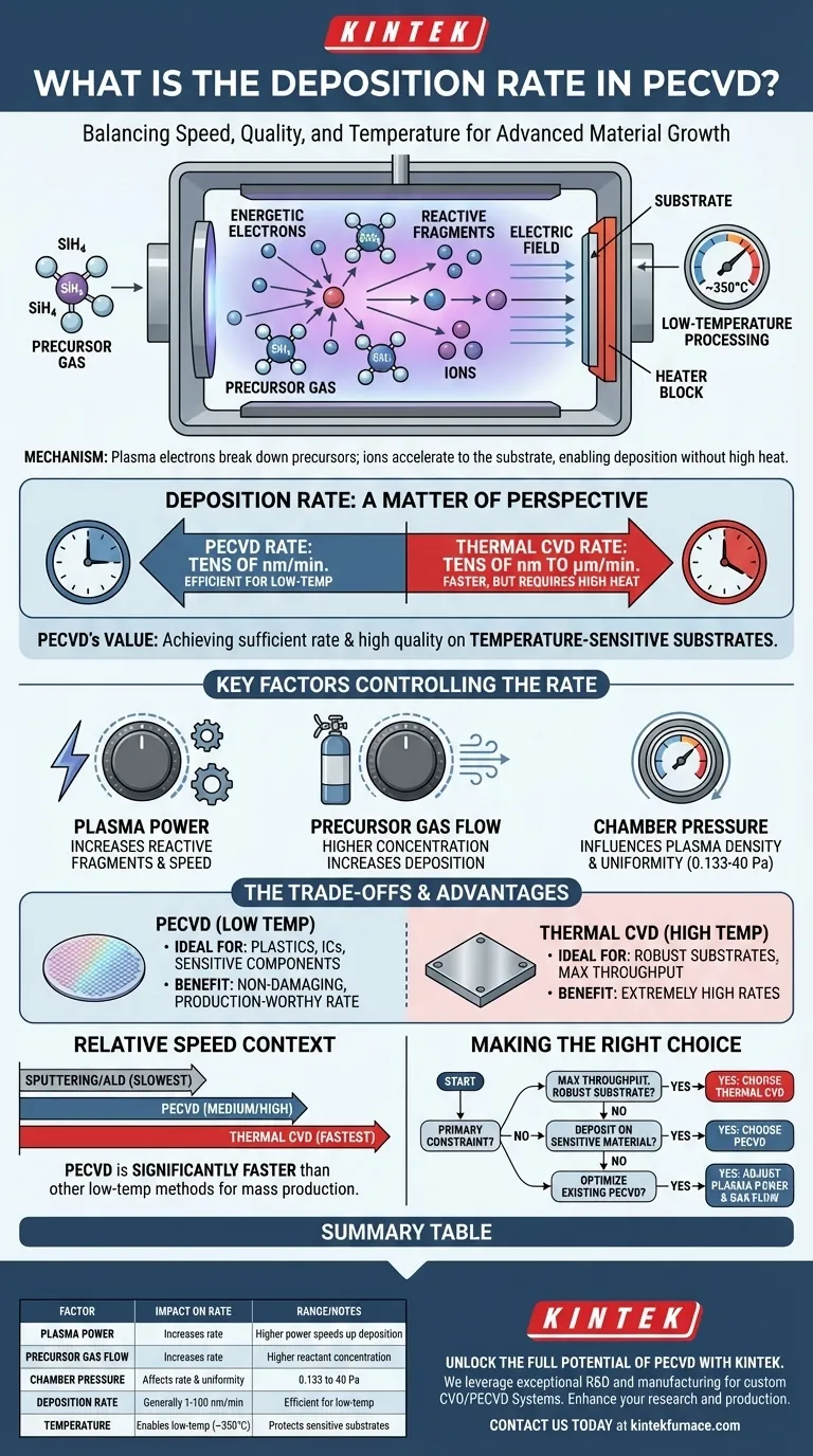
To be direct, the deposition rate of Plasma-Enhanced Chemical Vapor Deposition (PECVD) is a matter of perspective, often cited as a key advantage while being measurably slower than its high-temperature alternative, thermal CVD. Typical PECVD rates range from a few to tens of nanometers per minute. This rate is considered highly efficient because it is achieved at significantly lower temperatures, which is the primary reason for choosing the process.
PECVD's deposition rate is not its fastest attribute when compared to all other methods. Its true value lies in achieving a sufficiently fast and high-quality deposition at low temperatures, enabling the use of temperature-sensitive substrates that would be damaged by other processes.
The Mechanics of PECVD Deposition Rate
To understand the rate, you must first understand the mechanism. PECVD uses an electric field to generate plasma, which is a gas containing energized, ionized particles.
The Role of Plasma
The energy for the deposition reaction in PECVD comes from energetic electrons in the plasma, not from high heat.
These electrons collide with precursor gas molecules, breaking them down into reactive fragments. This allows the film-forming chemical reactions to occur at a much lower substrate temperature, typically around 350°C.
Furthermore, the plasma creates an electric field that accelerates ions toward the substrate. This energetic ion bombardment adds energy directly to the growing surface, further promoting dense, high-quality film growth without high heat.
Key Factors Controlling the Rate
You have direct control over several parameters that influence the deposition speed.
Plasma Power: Increasing the power of the plasma generates more reactive fragments from the precursor gas. This directly increases the availability of material for film formation, speeding up deposition.
Precursor Gas Flow: A higher flow rate of the precursor gas increases the concentration of reactants inside the chamber. With more material available to be activated by the plasma, the deposition rate naturally increases.
Chamber Pressure: The operating pressure, typically between 0.133 to 40 Pa, also plays a role. It influences the plasma density and the path of the reactive species, affecting both the rate and uniformity of the deposition.
Understanding the Trade-offs: Rate vs. Temperature
The discussion of deposition rate is meaningless without considering temperature. The choice between PECVD and other methods is almost always a trade-off between speed and the thermal budget of your substrate.
The PECVD Advantage: Low-Temperature Processing
The defining feature of PECVD is its ability to deposit high-quality films at low temperatures. This makes it an essential process for materials that cannot withstand high heat, such as plastics, integrated circuits with previous layers, or other sensitive components.
While its rate of "tens of nanometers per minute" seems modest, it is a highly effective rate for a low-temperature process.
The CVD Disadvantage: High-Temperature Requirement
Conventional thermal CVD operates at much higher temperatures. It relies on heat alone to break down precursor gases.
This thermal energy results in significantly higher deposition rates, often reaching tens of nanometers to several micrometers per minute. However, this speed comes at the cost of requiring a substrate that can tolerate extreme heat.
Why the "High Rate" Claim Exists
The claim that PECVD has a "high rate" is not incorrect; it is simply relative.
Compared to other low-temperature deposition techniques like sputtering or Atomic Layer Deposition (ALD), PECVD is significantly faster. For mass production of devices on temperature-sensitive wafers, its rate is high enough to be economically efficient and much faster than the alternatives.
Making the Right Choice for Your Goal
Your decision should be based on a clear understanding of your project's primary constraint.
- If your primary focus is maximum throughput on robust substrates: Thermal CVD is likely a better fit, provided your material can withstand the high processing temperatures.
- If your primary focus is depositing on temperature-sensitive materials: PECVD provides the optimal balance of a production-worthy deposition rate and a low-temperature, non-damaging process.
- If your primary focus is optimizing an existing PECVD process: Concentrate on systematically adjusting plasma power and precursor gas flow to increase your deposition rate without compromising film quality.
Understanding these principles allows you to select and optimize a deposition strategy that truly aligns with your technical and material requirements.
Summary Table:
| Factor | Impact on Deposition Rate | Typical Range/Notes |
|---|---|---|
| Plasma Power | Increases rate by generating more reactive fragments | Higher power speeds up deposition |
| Precursor Gas Flow | Increases rate with higher reactant concentration | Adjust flow for optimal material availability |
| Chamber Pressure | Affects rate and uniformity | 0.133 to 40 Pa, influences plasma density |
| Deposition Rate | Generally 1-100 nm/min | Efficient for low-temperature processes |
| Temperature | Enables low-temperature operation (~350°C) | Protects sensitive substrates |
Unlock the full potential of PECVD for your lab! At KINTEK, we leverage exceptional R&D and in-house manufacturing to provide advanced high-temperature furnace solutions, including our specialized CVD/PECVD Systems. With strong deep customization capabilities, we precisely meet unique experimental requirements for diverse laboratories. Whether you're working with temperature-sensitive substrates or need optimized deposition rates, our expertise ensures high-quality, efficient results. Contact us today to discuss how our PECVD systems can enhance your research and production processes!
Visual Guide
Related Products
- Slide PECVD Tube Furnace with Liquid Gasifier PECVD Machine
- RF PECVD System Radio Frequency Plasma Enhanced Chemical Vapor Deposition
- Inclined Rotary Plasma Enhanced Chemical Deposition PECVD Tube Furnace Machine
- Inclined Rotary Plasma Enhanced Chemical Deposition PECVD Tube Furnace Machine
- Multi Heating Zones CVD Tube Furnace Machine for Chemical Vapor Deposition Equipment
People Also Ask
- What are the advantages of using a tube furnace CVD system for Cu(111)/graphene? Superior Scalability and Quality
- What are the disadvantages of tube furnace cracking when processing heavy raw materials? Avoid Costly Downtime and Inefficiency
- How does a hydrogen reduction environment in an industrial tube furnace facilitate gold-copper alloy microspheres?
- In which industries is the tube furnace commonly used? Essential for Materials Science, Energy, and More
- What are the typical conditions for plasma-enhanced CVD processes? Achieve Low-Temperature Thin Film Deposition


