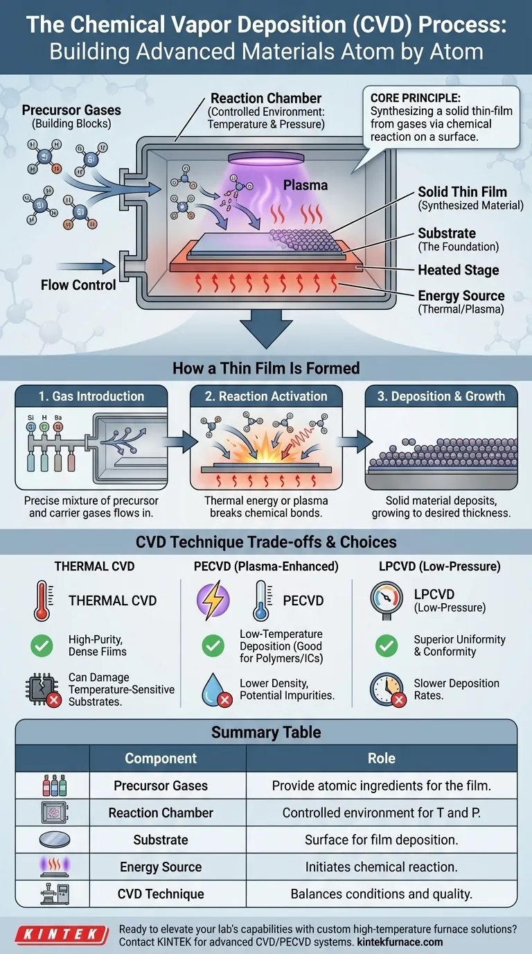
At its core, Chemical Vapor Deposition (CVD) is a manufacturing process that builds a solid, thin-film material onto a surface from the atoms and molecules within a gas. Precursor gases, which contain the chemical elements of the desired film, are introduced into a reaction chamber. By applying energy—typically in the form of heat—these gases undergo a chemical reaction that creates a new solid material, which then deposits evenly onto a target object, known as a substrate.
The fundamental principle of CVD is not merely coating a surface, but rather synthesizing a new, high-purity solid material directly onto it. This is achieved by precisely controlling a chemical reaction in the vapor phase, allowing for the construction of films with specific, engineered properties.

The Anatomy of the CVD Process
To understand how CVD works, it's essential to break it down into its four primary components. Each plays a critical role in the final quality of the deposited film.
The Precursor Gases (The Building Blocks)
Precursor gases are the volatile chemical compounds that carry the atomic ingredients for the final film. For example, to create a silicon film, a precursor like silane gas (SiH₄) might be used.
These gases are carefully selected based on the desired film composition and the required reaction conditions.
The Reaction Chamber (The Environment)
The entire process takes place within a sealed reaction chamber, which is typically a vacuum environment. This chamber allows for precise control over two critical variables: temperature and pressure.
Controlling this environment is non-negotiable for achieving a predictable and repeatable chemical reaction.
The Substrate (The Foundation)
The substrate is simply the object or material onto which the thin film is grown. This could be a silicon wafer for a microchip, a medical implant, or a cutting tool.
The substrate is heated to the target temperature, providing the energy and the surface needed for the deposition reaction to occur.
The Energy Source (The Catalyst for Reaction)
Energy is required to break the chemical bonds in the precursor gases and drive the reaction. Most commonly, this is thermal energy from heating the substrate to several hundred or even over a thousand degrees Celsius.
Alternatively, some CVD processes use an energy-rich plasma to initiate the reaction at much lower temperatures.
How a Thin Film Is Formed
The deposition process follows a clear sequence of events, transforming gas molecules into a solid, functional coating.
1. Introducing the Reactants
A precise mixture of precursor gases and carrier gases is flowed into the reaction chamber at a controlled rate.
2. Activating the Chemical Reaction
As the gases reach the hot substrate, they absorb thermal energy. This energy causes them to decompose or react with each other on the substrate's surface.
3. Deposition and Growth
The product of this chemical reaction is a solid material that is no longer stable in the gas phase. It deposits onto the hot substrate, forming a stable, solid thin film.
This process occurs layer by layer, allowing the film to grow to a desired thickness, which is controlled by deposition time and gas concentration.
Understanding the Trade-offs
The choice of CVD technique involves balancing temperature, pressure, and desired film quality. No single method is perfect for every application.
High Temperature vs. Material Integrity
Traditional thermal CVD produces very high-purity, dense films. However, its high temperature requirement can damage or destroy temperature-sensitive substrates, such as plastics or assembled electronic components.
The Solution: Plasma-Enhanced CVD (PECVD)
Plasma-Enhanced CVD (PECVD) uses an ionized gas (plasma) to provide the energy for the reaction. This allows deposition to occur at significantly lower temperatures.
The trade-off is that PECVD films may have lower density or incorporate impurities (like hydrogen) from the precursor gases, which can affect material properties.
Pressure and Uniformity: The LPCVD Advantage
Operating the reaction at low pressure, a technique known as Low-Pressure CVD (LPCVD), is a common strategy. It reduces unwanted chemical reactions in the gas phase, leading to fewer defects.
This results in films with superior thickness uniformity and the ability to coat complex, three-dimensional shapes evenly.
Making the Right Choice for Your Goal
Your choice of CVD method depends directly on your material and performance requirements. Understanding the core principles allows you to select the right tool for the job.
- If your primary focus is creating a highly pure, dense film on a temperature-resistant substrate: Standard thermal CVD or LPCVD provides the best crystalline quality and material properties.
- If your primary focus is coating a temperature-sensitive material like a polymer or an integrated circuit: PECVD is the necessary choice to avoid thermal damage to the underlying substrate.
- If your primary focus is achieving maximum uniformity across large surfaces or complex shapes: LPCVD offers superior film conformity by minimizing gas-phase reactions.
By mastering these variables, CVD transforms simple gases into highly engineered materials critical for modern technology.
Summary Table:
| Component | Role in CVD Process |
|---|---|
| Precursor Gases | Provide atomic ingredients for the film (e.g., silane for silicon) |
| Reaction Chamber | Controlled environment for temperature and pressure regulation |
| Substrate | Surface where the film is deposited (e.g., silicon wafers) |
| Energy Source | Initiates chemical reaction via heat or plasma |
| CVD Technique | Balances temperature, pressure, and film quality (e.g., PECVD for low temps, LPCVD for uniformity) |
Ready to elevate your lab's capabilities with custom high-temperature furnace solutions? At KINTEK, we leverage exceptional R&D and in-house manufacturing to provide advanced CVD/PECVD systems, Muffle, Tube, Rotary, Vacuum & Atmosphere Furnaces. Our deep customization ensures precise alignment with your unique experimental needs, whether you're developing microchips, medical implants, or other high-tech applications. Contact us today to discuss how our tailored solutions can drive your innovations forward!
Visual Guide
Related Products
- Custom Made Versatile CVD Tube Furnace Chemical Vapor Deposition CVD Equipment Machine
- MPCVD Machine System Reactor Bell-jar Resonator for Lab and Diamond Growth
- Multi Heating Zones CVD Tube Furnace Machine for Chemical Vapor Deposition Equipment
- 915MHz MPCVD Diamond Machine Microwave Plasma Chemical Vapor Deposition System Reactor
- Slide PECVD Tube Furnace with Liquid Gasifier PECVD Machine
People Also Ask
- What customization options are available for CVD tube furnaces? Tailor Your System for Superior Material Synthesis
- How can integrating CVD tube furnaces with other technologies benefit device fabrication? Unlock Advanced Hybrid Processes
- Which industries and research fields benefit from CVD tube furnace sintering systems for 2D materials? Unlock Next-Gen Tech Innovations
- How does CVD tube furnace sintering enhance graphene growth? Achieve Superior Crystallinity and High Electron Mobility
- What are the key features of CVD tube furnaces for 2D material processing? Unlock Precision Synthesis for Superior Materials


