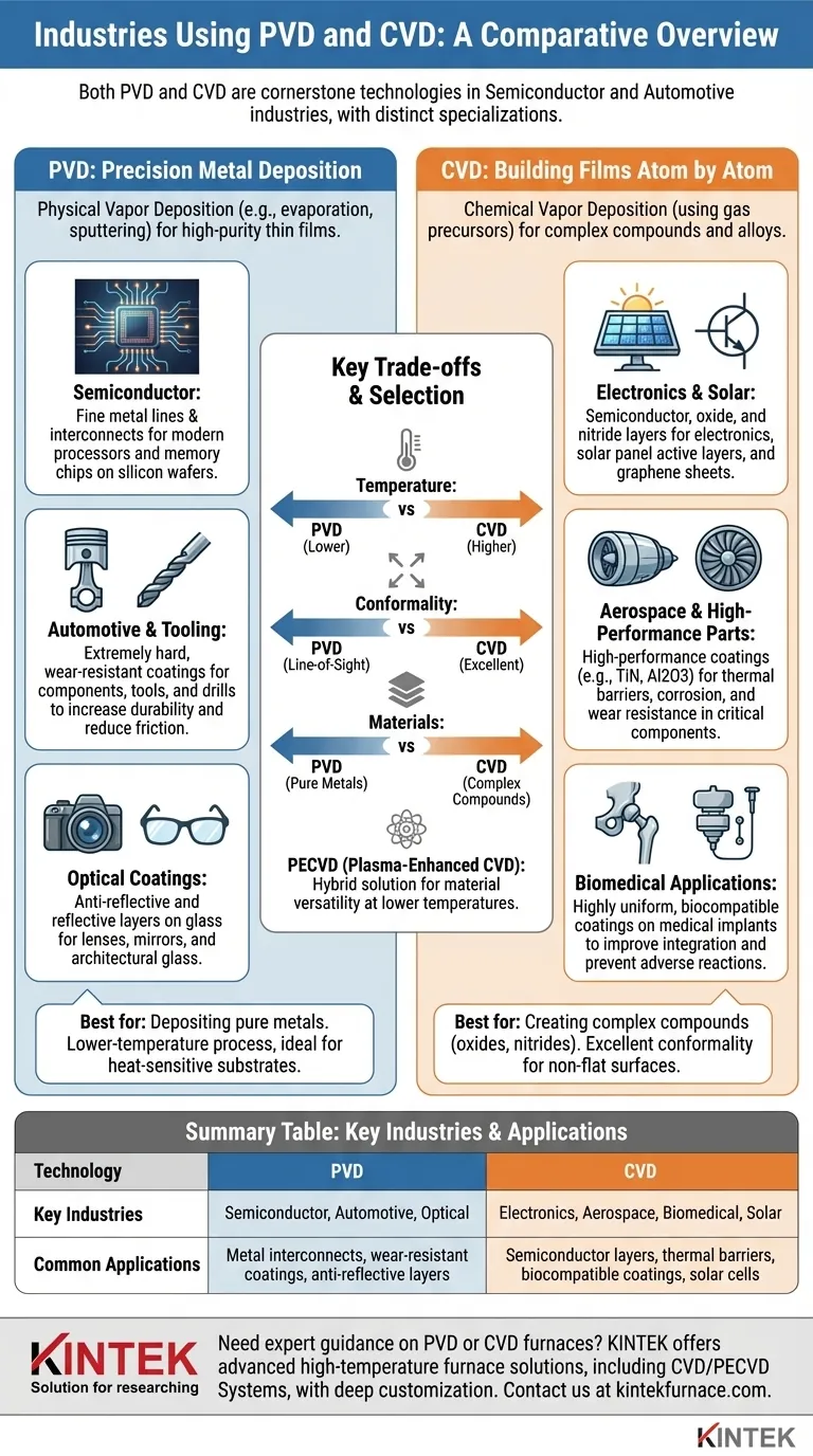
In short, both Physical Vapor Deposition (PVD) and Chemical Vapor Deposition (CVD) are cornerstone technologies in the semiconductor and automotive industries. PVD is also a mainstay for optical coatings, while CVD sees extensive and critical use in aerospace, biomedical applications, and solar panel manufacturing. The choice depends entirely on the material being deposited and the desired properties of the final film.
The decision between PVD and CVD is driven not by the industry, but by the application's specific material requirements. PVD is the go-to for depositing pure metals, while CVD offers superior versatility for creating complex compounds like oxides and nitrides with highly controlled properties.
Where PVD Shines: Precision Metal Deposition
Physical Vapor Deposition works by physically bombarding or evaporating a solid source material in a vacuum, causing it to travel and condense onto a substrate. This direct, line-of-sight process makes it exceptionally well-suited for depositing high-purity thin films, especially metals.
The Semiconductor Industry
In microelectronics, PVD is essential for creating the fine metal lines and interconnects that form the circuitry on a silicon wafer. Its precision is critical for building modern processors and memory chips.
Automotive and Tooling
PVD is used to apply extremely hard, wear-resistant coatings to engine components, tools, and drills. These thin metal films, often just a few microns thick, dramatically increase durability and reduce friction.
Optical Coatings
The process is widely used to deposit thin metallic and dielectric layers on glass. This creates the anti-reflective coatings on eyeglasses and camera lenses, as well as the reflective surfaces of mirrors and architectural glass.
The Versatility of CVD: Building Films Atom by Atom
Chemical Vapor Deposition is fundamentally different. It introduces precursor gases into a reaction chamber, which then chemically react and decompose on the substrate's surface to form the desired film. This allows for the creation of a vast range of materials beyond pure metals.
Electronics and Solar Industries
CVD is invaluable for depositing the semiconductor (e.g., silicon), oxide, and nitride layers that form transistors and other electronic components. It is also a key process in manufacturing the active layers of solar panels and even for producing high-quality graphene sheets for next-generation displays.
Aerospace and High-Performance Parts
The aerospace industry relies on CVD for high-performance coatings that provide thermal barriers and resistance to corrosion and wear. Materials like Titanium Nitride (TiN) and Aluminum Oxide (Al2O3) are common for protecting critical jet engine and structural components.
Biomedical Applications
CVD can create highly uniform, biocompatible coatings on medical implants. These films improve the device's integration with the body and prevent adverse reactions, making it a critical technology for modern medicine.
Understanding the Trade-offs
Choosing the correct deposition technology requires understanding their core operational differences and the resulting trade-offs in performance, material compatibility, and cost.
When to Choose PVD
PVD is typically a lower-temperature process than traditional CVD. This makes it ideal for coating substrates that cannot withstand high heat. If your goal is to deposit a pure metal with high precision, PVD is almost always the more straightforward and effective solution.
When to Choose CVD
CVD excels where PVD cannot. Its chemical nature allows it to deposit complex compounds and alloys with precise control over stoichiometry and structure. Furthermore, because it relies on gas diffusion, CVD provides excellent conformality, meaning it can uniformly coat highly complex, non-flat surfaces.
The Role of Plasma (PECVD)
Plasma-Enhanced Chemical Vapor Deposition (PECVD) is a crucial variant. It uses plasma to energize the precursor gases, allowing the chemical reaction to occur at much lower temperatures. This effectively bridges the gap, offering the material versatility of CVD on temperature-sensitive substrates where only PVD might have been an option.
Making the Right Choice for Your Application
Your final decision must be guided by the material you need to deposit and the functional requirements of the finished part.
- If your primary focus is depositing pure metals or working with heat-sensitive substrates: PVD is often the more direct and effective choice.
- If your goal is to create highly durable, conformal coatings of complex compounds like oxides or nitrides: CVD provides unmatched versatility and control over the film's properties.
- If you need the versatility of CVD but are constrained by lower process temperatures: Investigate Plasma-Enhanced CVD (PECVD) as the ideal hybrid solution.
Understanding the core mechanism—physical deposition versus a surface chemical reaction—is the key to selecting the right technology for your specific material and performance goals.
Summary Table:
| Technology | Key Industries | Common Applications |
|---|---|---|
| PVD | Semiconductor, Automotive, Optical | Metal interconnects, wear-resistant coatings, anti-reflective layers |
| CVD | Electronics, Aerospace, Biomedical, Solar | Semiconductor layers, thermal barriers, biocompatible coatings, solar cells |
Need expert guidance on selecting the right PVD or CVD furnace for your lab? At KINTEK, we leverage exceptional R&D and in-house manufacturing to provide advanced high-temperature furnace solutions, including Muffle, Tube, Rotary Furnaces, Vacuum & Atmosphere Furnaces, and CVD/PECVD Systems. Our strong deep customization capability ensures we can precisely meet your unique experimental requirements, enhancing efficiency and performance. Contact us today to discuss how our tailored solutions can benefit your industry application!
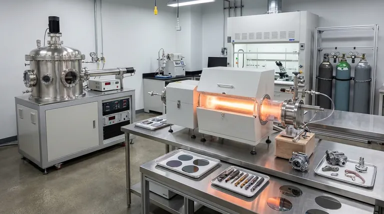
Visual Guide
Related Products
- HFCVD Machine System Equipment for Drawing Die Nano Diamond Coating
- Custom Made Versatile CVD Tube Furnace Chemical Vapor Deposition CVD Equipment Machine
- RF PECVD System Radio Frequency Plasma Enhanced Chemical Vapor Deposition
- Multi Heating Zones CVD Tube Furnace Machine for Chemical Vapor Deposition Equipment
- Split Chamber CVD Tube Furnace with Vacuum Station CVD Machine
People Also Ask
- What is Hot-filament Chemical Vapor Deposition (HFCVD)? Achieve High-Quality Thin Films with Precision Control
- What is the function of high-purity Argon (Ar) gas during CVD? Optimize Your Thin Film Uniformity and Purity
- What materials are commonly used in CVD coating systems? Explore Key Materials for Superior Coatings
- How can customers maximize the quality of CVD coatings? Master Pre-Coating Prep for Superior Results
- What is the advantage of using a CVD system for coating turbine blades? Master Complex Geometries with Ease


