To enhance the bonding force of a gate dielectric film, you must focus on two primary areas within your CVD tube furnace process. The first is the rigorous optimization of deposition parameters—specifically temperature, pressure, and gas flow ratios—to control film growth at the atomic level. The second is the implementation of a deliberate post-deposition annealing step to densify the film and chemically strengthen the dielectric-substrate interface.
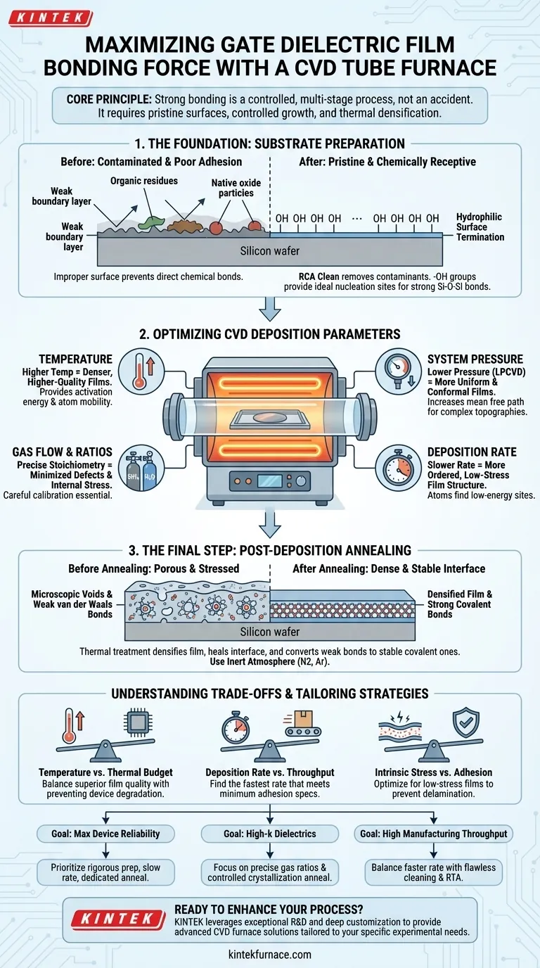
The core principle is that a strong bond is not an accident of deposition, but the result of a controlled, multi-stage process. True adhesion comes from creating a pristine, chemically receptive substrate surface and then managing the thermal and chemical environment to form a dense, low-stress film with a stable interface.
The Foundation: Substrate Preparation
Before any deposition begins, the state of the substrate surface dictates the ultimate bonding potential. An improperly prepared surface is the most common and preventable cause of film delamination.
The Critical Role of Surface Cleaning
All effective bonding starts with an impeccably clean surface. Contaminants create a weak boundary layer that prevents the dielectric film from forming direct, strong chemical bonds with the substrate.
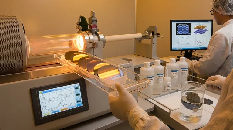
You must employ a multi-step cleaning sequence, such as the RCA clean for silicon wafers, to systematically remove organic residues, ionic contaminants, and native oxides.
Surface Termination for Chemical Bonding
A clean surface is not enough; it must also be chemically receptive. The goal is to "terminate" the surface with a uniform layer of functional groups that will readily react with the CVD precursors.
For silicon dioxide (SiO₂) deposition on silicon, for example, creating a hydrophilic surface covered in hydroxyl (-OH) groups provides ideal nucleation sites for the film to grow, promoting strong Si-O-Si bonds at the interface.
Optimizing CVD Deposition Parameters
The conditions inside the CVD tube furnace during film growth have a direct impact on the film's intrinsic properties and its adhesion to the substrate.
Deposition Temperature
Temperature is arguably the most critical parameter. It provides the activation energy for surface reactions and controls the mobility of deposited atoms.
Higher temperatures generally yield denser, higher-quality films with better adhesion. However, this must be balanced against the device's overall thermal budget.
System Pressure
Pressure influences the mean free path of gas molecules. Lower pressures (LPCVD) increase the mean free path, leading to more uniform and conformal films, which is critical for adhesion over complex topographies.
This uniformity ensures that stress is distributed evenly and prevents localized weak points at sharp corners or steps.
Precursor Gas Flow and Ratios
The ratio of precursor gases determines the stoichiometry of the final film. An off-stoichiometry film (e.g., silicon-rich or oxygen-rich oxide) contains more defects and inherent stress.
Careful calibration of mass flow controllers is essential to achieve a film that is as close to its ideal chemical composition as possible, as this minimizes internal stress and promotes a stable interface.
Deposition Rate
A slower deposition rate generally improves bonding force. It gives adsorbed atoms more time to migrate across the surface and find low-energy lattice sites, resulting in a more ordered and less stressed film structure.
Understanding the Trade-offs
Optimizing for bonding force often requires balancing competing factors. Acknowledging these trade-offs is key to developing a robust and practical process.
Temperature vs. Thermal Budget
While high temperatures create superior films, they can also cause unwanted diffusion of dopants from underlying layers or damage temperature-sensitive structures. The optimal temperature is often the highest one the device can tolerate without degradation.
Deposition Rate vs. Throughput
A slow deposition rate that is ideal for adhesion directly conflicts with the need for high manufacturing throughput. The practical solution is to find the fastest rate that still meets the minimum adhesion and reliability specifications for the device.
Intrinsic Film Stress vs. Adhesion
All thin films have some level of intrinsic stress from the deposition process. While a strong chemical bond provides adhesion, excessive tensile or compressive stress in the film can physically pull it apart from the substrate, causing delamination. Optimizing parameters to achieve a low-stress film is therefore a direct method of improving effective bonding.
The Final Step: Post-Deposition Annealing
Annealing is a high-temperature treatment performed after deposition and is one of the most effective ways to improve the bonding and overall quality of the dielectric film.
How Annealing Densifies the Film
The thermal energy from annealing allows atoms within the film to rearrange into a more ordered, lower-energy state. This process reduces microscopic voids and increases the film's density, making it mechanically stronger and less permeable.
Healing the Dielectric-Substrate Interface
Annealing can promote chemical reactions at the interface, transforming weaker van der Waals bonds into stronger, more stable covalent bonds. It also helps reduce the density of electronic trap states at the interface, which is critical for transistor performance.
Choosing the Annealing Atmosphere
The gas used during annealing matters. Annealing in an inert atmosphere like Nitrogen (N₂) or Argon (Ar) primarily drives densification. Annealing in a reactive atmosphere like Oxygen (O₂) can help consume carbon impurities but may also grow an unwanted interfacial layer.
Making the Right Choice for Your Goal
Your optimization strategy should be guided by your end application.
- If your primary focus is maximum device reliability: Prioritize rigorous surface preparation, a slow deposition rate, and a dedicated post-deposition anneal to create the most stable film possible.
- If your primary focus is high-k dielectrics: Concentrate on precise gas flow ratios to control stoichiometry and use a carefully controlled anneal to crystallize the film and heal the complex interface with the silicon substrate.
- If your primary focus is high manufacturing throughput: Find a balance by slightly increasing the deposition rate while ensuring your surface cleaning is flawless and implementing a rapid thermal anneal (RTA) as an efficient post-processing step.
Ultimately, achieving a superior bonding force is about exercising precise control over every stage of the film's creation.
Summary Table:
| Aspect | Key Improvements |
|---|---|
| Substrate Preparation | Use RCA cleaning and hydrophilic surface termination for strong chemical bonds. |
| Deposition Parameters | Optimize temperature, pressure, gas ratios, and deposition rate for low-stress films. |
| Post-Deposition Annealing | Apply annealing in inert atmospheres to densify films and strengthen interfaces. |
| Trade-offs | Balance temperature vs. thermal budget and deposition rate vs. throughput. |
Ready to enhance your gate dielectric film bonding? At KINTEK, we leverage exceptional R&D and in-house manufacturing to provide advanced high-temperature furnace solutions tailored for your lab. Our product line includes Muffle, Tube, Rotary Furnaces, Vacuum & Atmosphere Furnaces, and CVD/PECVD Systems, with strong deep customization capabilities to precisely meet your unique experimental needs. Contact us today to discuss how our expertise can improve your device reliability and throughput!
Visual Guide
Related Products
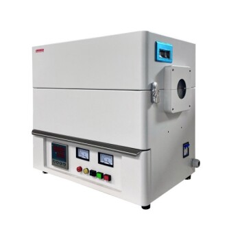
- Custom Made Versatile CVD Tube Furnace Chemical Vapor Deposition CVD Equipment Machine
- Split Chamber CVD Tube Furnace with Vacuum Station CVD Machine
- Multi Heating Zones CVD Tube Furnace Machine for Chemical Vapor Deposition Equipment
- Slide PECVD Tube Furnace with Liquid Gasifier PECVD Machine
- Inclined Rotary Plasma Enhanced Chemical Deposition PECVD Tube Furnace Machine
People Also Ask
- How does CVD tube furnace sintering enhance graphene growth? Achieve Superior Crystallinity and High Electron Mobility
- What future trends are expected in the development of CVD tube furnaces? Discover Smarter, More Versatile Systems
- Why are CVD tube furnace sintering systems indispensable for 2D material research and production? Unlock Atomic-Scale Precision
- What are the practical applications of gate media prepared by CVD tube furnaces? Unlock Advanced Electronics and More
- What is a CVD tube furnace and what is its primary function? Discover Precision Thin-Film Deposition