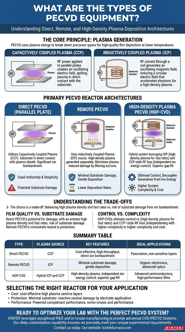
The primary types of PECVD equipment are distinguished by how they generate and apply plasma to the substrate. These architectures are broadly classified as Direct PECVD, which uses a Capacitively Coupled Plasma (CCP), Remote PECVD, which uses an Inductively Coupled Plasma (ICP), and High-Density Plasma (HDP-CVD) systems, which combine both methods for advanced control.
The choice between PECVD systems is fundamentally a trade-off. You are balancing the need for high plasma density and fast deposition rates against the risk of substrate damage from energetic ion bombardment. Your specific application dictates which balance is correct.
The Core Principle: Plasma Generation
At its heart, Plasma-Enhanced Chemical Vapor Deposition (PECVD) is a process that uses energy from a plasma to break down precursor gases into reactive species. This allows for the deposition of high-quality thin films at significantly lower temperatures than traditional Chemical Vapor Deposition (CVD), protecting sensitive substrates.
Capacitively Coupled Plasma (CCP)
CCP is one of the most common methods for generating plasma. It functions much like a capacitor, with the substrate placed on one of two parallel metal plates.
An RF (Radio Frequency) power source is applied to the plates, creating an oscillating electric field that ignites and sustains the plasma in the space between them, in direct contact with the substrate.
Inductively Coupled Plasma (ICP)
ICP uses a different principle to energize the gas. An RF current is passed through a coil, typically wrapped around a dielectric chamber wall.
This current generates an oscillating magnetic field, which in turn induces a circular electric field inside the chamber. This electric field accelerates electrons and creates a very dense, high-concentration plasma.
Primary PECVD Reactor Architectures
The way these plasma sources are integrated into a vacuum chamber defines the main types of PECVD equipment.
Direct PECVD (Parallel Plate)
This is the classic PECVD configuration, utilizing a Capacitively Coupled Plasma (CCP). The substrate sits directly within the plasma generated between two parallel electrodes.
Because the substrate is in direct contact with the plasma sheath, it experiences significant ion bombardment. This can be beneficial for creating dense films but may also cause damage to sensitive electronic or optical materials.
Remote PECVD
These systems are designed specifically to minimize plasma-induced damage. They use an Inductively Coupled Plasma (ICP) source to generate a high-density plasma in a region separate from the substrate.
The reactive neutral species then flow or diffuse from the remote plasma zone to the substrate, while the charged ions are largely filtered out. This results in a gentler deposition process ideal for delicate materials.
High-Density Plasma PECVD (HDP-CVD)
HDP-CVD represents the most advanced and versatile architecture. It is a hybrid system that leverages the strengths of both plasma generation methods.
It typically uses an ICP source to generate a very high-density plasma, enabling fast deposition rates and efficient gas dissociation. Simultaneously, it uses a separate CCP-style RF bias on the substrate holder to independently control the energy of ions arriving at the surface. This dual control allows for superior gap-fill capabilities in microelectronics and the deposition of very high-quality films.
Understanding the Trade-offs
No single PECVD system is universally superior. The optimal choice depends on balancing performance requirements against potential drawbacks.
Film Quality vs. Substrate Damage
Direct PECVD (CCP) systems provide good uniformity and are mechanically simple. However, the direct ion bombardment can be a significant source of damage for sensitive device layers.
Remote PECVD excels at protecting the substrate, making it the go-to choice for applications where any plasma damage is unacceptable. This gentleness, however, can sometimes come at the cost of lower deposition rates.
Control vs. Complexity
HDP-CVD offers the ultimate control, decoupling plasma generation from ion energy. This allows engineers to fine-tune film properties like stress and density while maintaining high deposition rates. This performance, however, comes with significantly higher system complexity and cost.
Selecting the Right Reactor for Your Application
Your decision should be driven by the primary goal of your deposition process.
- If your primary focus is cost-effective, high-throughput deposition for non-sensitive layers (e.g., passivation): Direct PECVD (CCP) offers the most straightforward and economical solution.
- If your primary focus is depositing films on delicate materials where damage is the main concern (e.g., organic electronics, advanced optics): Remote PECVD provides the necessary protection for the substrate.
- If your primary focus is maximum performance for demanding applications (e.g., trench filling in advanced semiconductors): HDP-CVD provides the independent control over plasma density and ion energy required for superior results.
By understanding these fundamental designs, you can select the precise tool needed to achieve your specific material deposition goals.
Summary Table:
| Type | Plasma Source | Key Features | Ideal Applications |
|---|---|---|---|
| Direct PECVD | Capacitively Coupled Plasma (CCP) | Cost-effective, high-throughput, direct ion bombardment | Passivation, non-sensitive layers |
| Remote PECVD | Inductively Coupled Plasma (ICP) | Minimal substrate damage, gentle deposition | Organic electronics, advanced optics |
| HDP-CVD | Hybrid ICP and CCP | High-density plasma, independent ion energy control, superior gap-fill | Advanced semiconductors, high-performance films |
Ready to optimize your lab with the perfect PECVD system? KINTEK leverages exceptional R&D and in-house manufacturing to provide advanced high-temperature furnace solutions, including CVD/PECVD Systems. Our strong deep customization capability ensures we precisely meet your unique experimental requirements. Contact us today to discuss how our tailored solutions can enhance your material deposition processes!
Visual Guide
Related Products
- Slide PECVD Tube Furnace with Liquid Gasifier PECVD Machine
- Inclined Rotary Plasma Enhanced Chemical Deposition PECVD Tube Furnace Machine
- Inclined Rotary Plasma Enhanced Chemical Deposition PECVD Tube Furnace Machine
- RF PECVD System Radio Frequency Plasma Enhanced Chemical Vapor Deposition
- Multi Heating Zones CVD Tube Furnace Machine for Chemical Vapor Deposition Equipment
People Also Ask
- How does a hydrogen reduction environment in an industrial tube furnace facilitate gold-copper alloy microspheres?
- What are the typical conditions for plasma-enhanced CVD processes? Achieve Low-Temperature Thin Film Deposition
- What are the main advantages of PECVD tube furnaces compared to CVD tube furnaces? Lower Temp, Faster Deposition, and More
- How does PECVD equipment contribute to TOPCon bottom cells? Mastering Hydrogenation for Maximum Solar Efficiency
- What is plasma in the context of PECVD? Unlock Low-Temperature Thin Film Deposition


