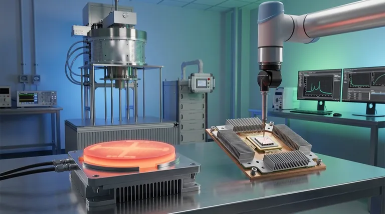
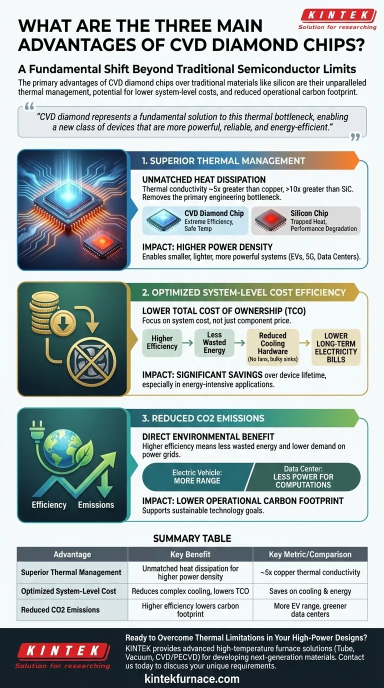
The primary advantages of CVD diamond chips over traditional semiconductor materials like silicon are their unparalleled thermal management capabilities, potential for lower system-level costs, and a significantly reduced operational carbon footprint. These three benefits directly address the growing limitations of silicon in high-power and high-frequency applications, paving the way for more efficient and compact electronic systems.
While silicon-based semiconductors have been the backbone of modern electronics, they are approaching their physical limits, particularly in managing waste heat. CVD diamond represents a fundamental solution to this thermal bottleneck, enabling a new class of devices that are more powerful, reliable, and energy-efficient.
Advantage 1: Superior Thermal Management
The most significant advantage of diamond is its ability to dissipate heat more effectively than any other semiconductor material.
Why Heat is the Bottleneck
In power electronics, inefficiency manifests as waste heat. As devices become smaller and more powerful, concentrating and removing this heat becomes the primary engineering challenge. Excessive heat degrades performance, reduces reliability, and ultimately limits the power a device can handle.
Diamond's Unmatched Thermal Conductivity
Diamond has the highest known thermal conductivity of any bulk material, approximately 5 times greater than copper and over 10 times greater than silicon carbide (SiC).
This means a CVD diamond chip can pull heat away from active electronic components with extreme efficiency, keeping the device operating at a safe and optimal temperature.
The Practical Impact: Higher Power Density
Because heat is managed so effectively, engineers can design components that handle much more power in the same physical space. This leads to higher power density, enabling smaller, lighter, and more powerful systems—a critical factor in electric vehicles, 5G infrastructure, and data centers.
Advantage 2: Optimized System-Level Cost Efficiency
While diamond as a raw material can be expensive, its use in semiconductors can lead to significant cost savings at the system level. This is a crucial distinction from initial component cost.
The Misconception of Component Cost
Focusing solely on the price of the chip is misleading. The true cost of a system includes cooling hardware, passive components, and the energy it consumes over its lifetime.
How Efficiency Reduces Total Cost of Ownership (TCO)
Diamond-based electronics operate more efficiently, wasting far less energy as heat. This reduces the need for bulky and expensive cooling systems like fans, heat sinks, and liquid cooling loops.
Over the device's operational life, the dramatic reduction in wasted energy translates directly into lower electricity bills—a major factor for energy-intensive applications like data centers.
Advantage 3: Reduced CO2 Emissions
The superior efficiency of CVD diamond has a direct and positive environmental impact by lowering the carbon footprint of electronic systems.
The Direct Link Between Efficiency and Emissions
Every kilowatt-hour of energy wasted by an inefficient electronic device contributes to unnecessary carbon emissions from power generation. By minimizing this waste, diamond-based systems reduce the overall demand on the power grid.
For an electric vehicle, this means more range from the same battery. For a data center, it means performing more computations with less power, directly reducing its operational carbon footprint.
Understanding the Trade-offs
No material is a universal solution. It's important to recognize the current challenges associated with CVD diamond.
Manufacturing Complexity
Growing high-quality, electronics-grade diamond films using Chemical Vapor Deposition (CVD) is a complex and capital-intensive process. While scaling is improving, initial manufacturing costs remain a significant hurdle compared to the mature silicon industry.
System Integration and Ecosystem
Silicon has a multi-trillion-dollar ecosystem built around it over 60 years. Integrating a new material like diamond requires new design rules, fabrication techniques, and a supply chain that is still in its infancy. This makes development cycles longer and more specialized.
Application Specificity
CVD diamond's benefits are most pronounced in high-power, high-frequency, and thermally demanding applications. It is not a cost-effective replacement for the low-power logic chips found in a typical computer or smartphone. Its value is in solving specific, high-stakes problems that other materials cannot.
Making the Right Choice for Your Goal
The decision to use CVD diamond depends entirely on your primary objective.
- If your primary focus is maximum power density and reliability: For demanding applications like military radar or satellite communications, CVD diamond's thermal properties provide an unmatched performance advantage.
- If your primary focus is energy efficiency and long-term operating costs: For power-hungry systems like EV inverters or data center power supplies, the TCO savings from diamond's efficiency can justify the higher initial investment.
- If your primary focus is balancing cost for mass-market applications: For now, established materials like silicon, GaN, and SiC often provide a more pragmatic balance of performance and cost for consumer-grade products.
By understanding its unique strengths, you can identify where this next-generation material will deliver a decisive engineering and commercial advantage.
Summary Table:
| Advantage | Key Benefit | Key Metric/Comparison |
|---|---|---|
| Superior Thermal Management | Unmatched heat dissipation for higher power density | Thermal conductivity ~5x greater than copper |
| Optimized System-Level Cost | Reduces need for complex cooling, lowers Total Cost of Ownership (TCO) | Saves on cooling hardware & long-term energy costs |
| Reduced CO2 Emissions | Higher efficiency directly lowers operational carbon footprint | Enables more range for EVs, less power for data centers |
Ready to Overcome Thermal Limitations in Your High-Power Designs?
Leveraging exceptional R&D and in-house manufacturing, KINTEK provides innovators in power electronics, EV, and telecommunications with advanced high-temperature furnace solutions crucial for developing next-generation materials like CVD diamond.
Our product line—including Tube Furnaces, Vacuum & Atmosphere Furnaces, and CVD/PECVD Systems—is complemented by strong deep customization capabilities to precisely meet your unique material synthesis and research requirements.
Contact us today to discuss how our solutions can help you achieve superior thermal management and efficiency in your applications.
Visual Guide
Related Products
- 915MHz MPCVD Diamond Machine Microwave Plasma Chemical Vapor Deposition System Reactor
- Cylindrical Resonator MPCVD Machine System for Lab Diamond Growth
- HFCVD Machine System Equipment for Drawing Die Nano Diamond Coating
- MPCVD Machine System Reactor Bell-jar Resonator for Lab and Diamond Growth
- Custom Made Versatile CVD Tube Furnace Chemical Vapor Deposition CVD Equipment Machine
People Also Ask
- What factors influence the quality of diamond deposition in the MPCVD method? Master the Critical Parameters for High-Quality Diamond Growth
- What are the essential components of an MPCVD reactor for diamond film deposition? Unlock High-Quality Diamond Growth
- What is the MPCVD method and why is it considered effective for diamond deposition? Superior Purity & High Growth Rates
- What are some key features and benefits of the microwave plasma chemical vapor deposition system? Achieve Unmatched Material Synthesis
- In which industries is the microwave plasma chemical vapor deposition system commonly used? Unlock High-Purity Material Synthesis


