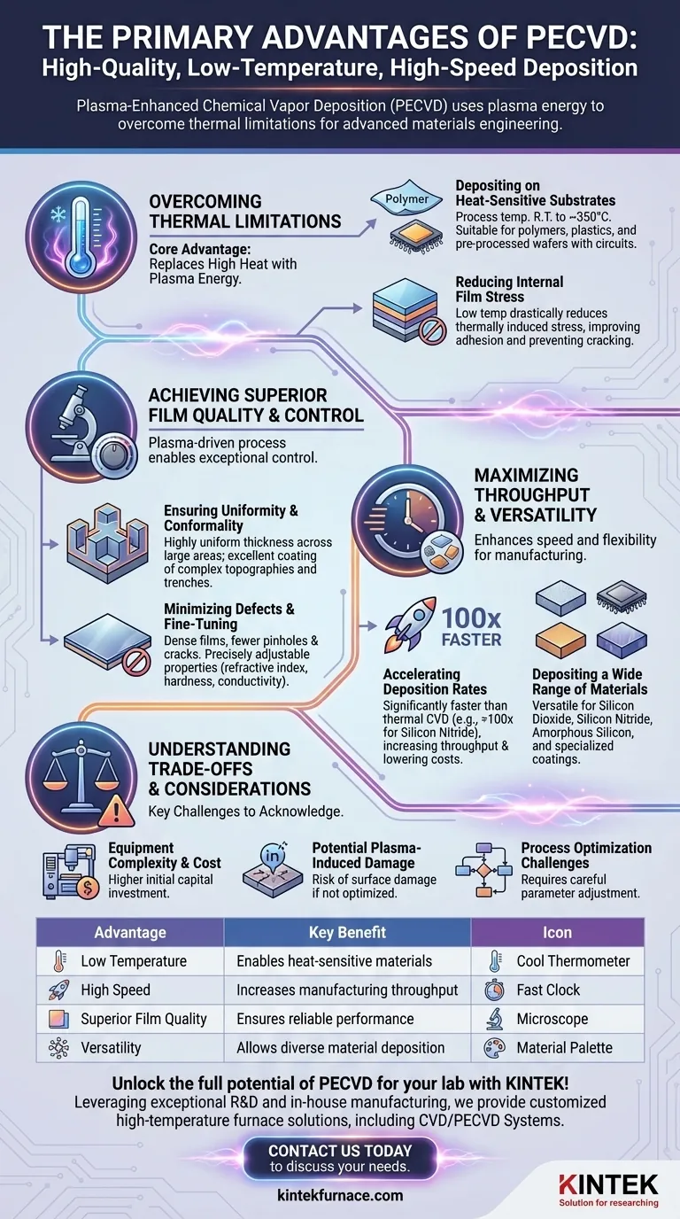
In short, the primary advantages of PECVD are its ability to deposit high-quality thin films at low temperatures and high speeds. This combination overcomes the major limitations of conventional thermal Chemical Vapor Deposition (CVD), enabling the coating of heat-sensitive materials and significantly increasing manufacturing throughput without sacrificing the integrity of the final film.
PECVD's core value lies in its use of plasma to energize chemical reactions, replacing the need for high heat. This fundamental shift allows for faster, cooler, and more controlled deposition, making it an indispensable tool for modern semiconductor fabrication and advanced materials engineering.
The Core Advantage: Overcoming Thermal Limitations
Traditional CVD processes rely on high temperatures (often >600°C) to provide the energy needed for chemical reactions to occur on a substrate surface. PECVD sidesteps this requirement by using an electric field to create plasma, a state of energized gas. This plasma provides the necessary energy, unlocking two critical benefits.
Depositing on Heat-Sensitive Substrates
The most significant advantage of PECVD is its low deposition temperature, typically ranging from room temperature to around 350°C.
This makes it possible to deposit films on materials that would be damaged or destroyed by the high heat of conventional CVD. This includes polymers, plastics, and fully fabricated semiconductor wafers with pre-existing metallic circuits.
Reducing Internal Film Stress
When depositing multiple layers of different materials, a mismatch in their thermal expansion coefficients can create significant stress during high-temperature processing. This leads to cracking, delamination, and poor device performance.
Because PECVD operates at low temperatures, it drastically reduces this thermally induced stress. The result is superior film adhesion and better electrical and mechanical integrity, especially in complex multi-layer structures.
Achieving Superior Film Quality and Control
The plasma-driven process not only allows for lower temperatures but also provides an exceptional degree of control over the film's final characteristics.
Ensuring Uniformity and Conformality
PECVD is renowned for producing films of highly uniform thickness across large-area substrates, such as silicon wafers.
It also provides excellent conformality, meaning it can evenly coat complex, three-dimensional topographies and high-aspect-ratio trenches. This is critical for creating reliable interconnects and insulating layers in microelectronics.
Minimizing Defects like Pinholes and Cracks
The low-stress environment and controlled reaction kinetics of PECVD result in films with significantly fewer defects. The deposited layers are dense, with a low incidence of pinholes and a reduced tendency to crack, leading to more robust and reliable device performance.
Fine-Tuning Material Properties
The plasma environment offers multiple variables that can be precisely adjusted, including gas composition, pressure, power, and frequency.
This allows engineers to fine-tune specific film properties such as its refractive index, hardness, chemical resistance, and electrical conductivity to meet the exact requirements of an application.
Maximizing Throughput and Versatility
Beyond quality, PECVD offers significant practical advantages in a manufacturing context, enhancing both speed and flexibility.
Accelerating Deposition Rates
The plasma significantly enhances chemical reaction rates, allowing for deposition speeds that can be orders of magnitude faster than conventional CVD. For materials like silicon nitride, PECVD can be over 100 times faster.
This dramatic increase in speed translates directly to higher manufacturing throughput and lower cost per unit.
Depositing a Wide Range of Materials
PECVD is an incredibly versatile technique capable of depositing a broad spectrum of materials. This includes dielectrics (silicon dioxide, silicon nitride), semiconductors (amorphous silicon), conductive films, and even specialized polymers.
Enabling Large-Area and Thick-Film Deposition
The process scales well for coating large substrates and is also capable of depositing thick coatings (often greater than 10 μm), a task that is difficult or impossible with many conventional thermal deposition methods.
Understanding the Trade-offs and Considerations
While powerful, PECVD is not without its complexities. Acknowledging these is key to successful implementation.
Equipment Complexity and Cost
A PECVD system, with its vacuum chamber, RF power source, and gas handling systems, is inherently more complex and expensive than a simple thermal CVD furnace. This represents a higher initial capital investment.
Potential for Plasma-Induced Damage
The high-energy ions within the plasma can, if not properly controlled, cause physical or electrical damage to the substrate surface or underlying device layers. Optimizing the process to mitigate this damage is a critical consideration for sensitive applications.
Process Optimization Challenges
The same variables that give PECVD its versatility also create a complex parameter space. Achieving a desired film property requires careful optimization of multiple interdependent factors, which can be a time-consuming development process.
Making the Right Choice for Your Application
Selecting the right deposition method depends entirely on your project's constraints and goals.
- If your primary focus is manufacturing speed and throughput: PECVD's high deposition rates offer a clear advantage over slower thermal processes, making it ideal for high-volume production.
- If you are working with temperature-sensitive materials: The low operating temperature of PECVD is its most defining and non-negotiable benefit, enabling deposition on polymers or pre-processed wafers.
- If your goal is to create high-quality, defect-free functional layers: PECVD offers exceptional control over film stress, uniformity, and adhesion, making it a superior choice for robust electronic and optical devices.
- If you require highly specialized film properties: The ability to precisely tune material characteristics by adjusting plasma parameters gives PECVD unmatched versatility for advanced research and development.
By understanding these core advantages, you can confidently determine when PECVD is the optimal tool to achieve your material engineering goals.
Summary Table:
| Advantage | Key Benefit |
|---|---|
| Low Temperature | Enables deposition on heat-sensitive materials like polymers and pre-processed wafers |
| High Speed | Increases manufacturing throughput with faster deposition rates |
| Superior Film Quality | Ensures uniformity, conformality, and minimal defects for reliable performance |
| Versatility | Allows deposition of various materials and fine-tuning of film properties |
Unlock the full potential of PECVD for your lab with KINTEK! Leveraging exceptional R&D and in-house manufacturing, we provide advanced high-temperature furnace solutions, including CVD/PECVD Systems, tailored to your unique experimental needs. Our deep customization capabilities ensure precise performance for semiconductor fabrication and materials engineering. Contact us today to discuss how our PECVD systems can enhance your research and production efficiency!
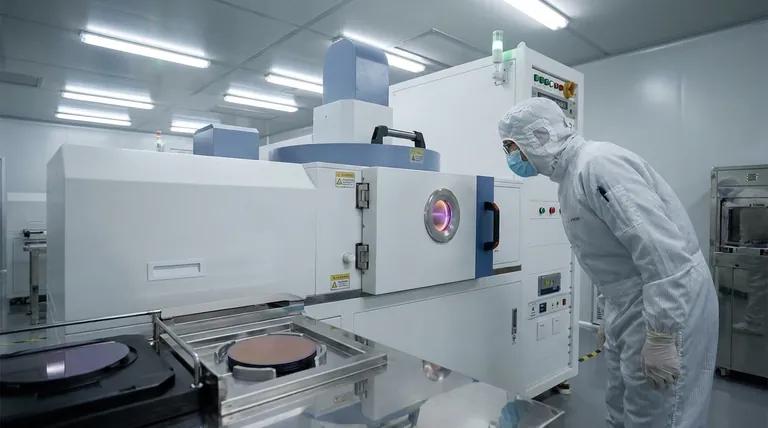
Visual Guide
Related Products
- Slide PECVD Tube Furnace with Liquid Gasifier PECVD Machine
- RF PECVD System Radio Frequency Plasma Enhanced Chemical Vapor Deposition
- Inclined Rotary Plasma Enhanced Chemical Deposition PECVD Tube Furnace Machine
- Inclined Rotary Plasma Enhanced Chemical Deposition PECVD Tube Furnace Machine
- Multi Heating Zones CVD Tube Furnace Machine for Chemical Vapor Deposition Equipment
People Also Ask
- What plasma source is used in PE-CVD tube furnaces? Unlock Low-Temperature, High-Quality Deposition
- How does a hydrogen reduction environment in an industrial tube furnace facilitate gold-copper alloy microspheres?
- How does PECVD equipment contribute to TOPCon bottom cells? Mastering Hydrogenation for Maximum Solar Efficiency
- What are the main advantages of PECVD tube furnaces compared to CVD tube furnaces? Lower Temp, Faster Deposition, and More
- What are the disadvantages of tube furnace cracking when processing heavy raw materials? Avoid Costly Downtime and Inefficiency


