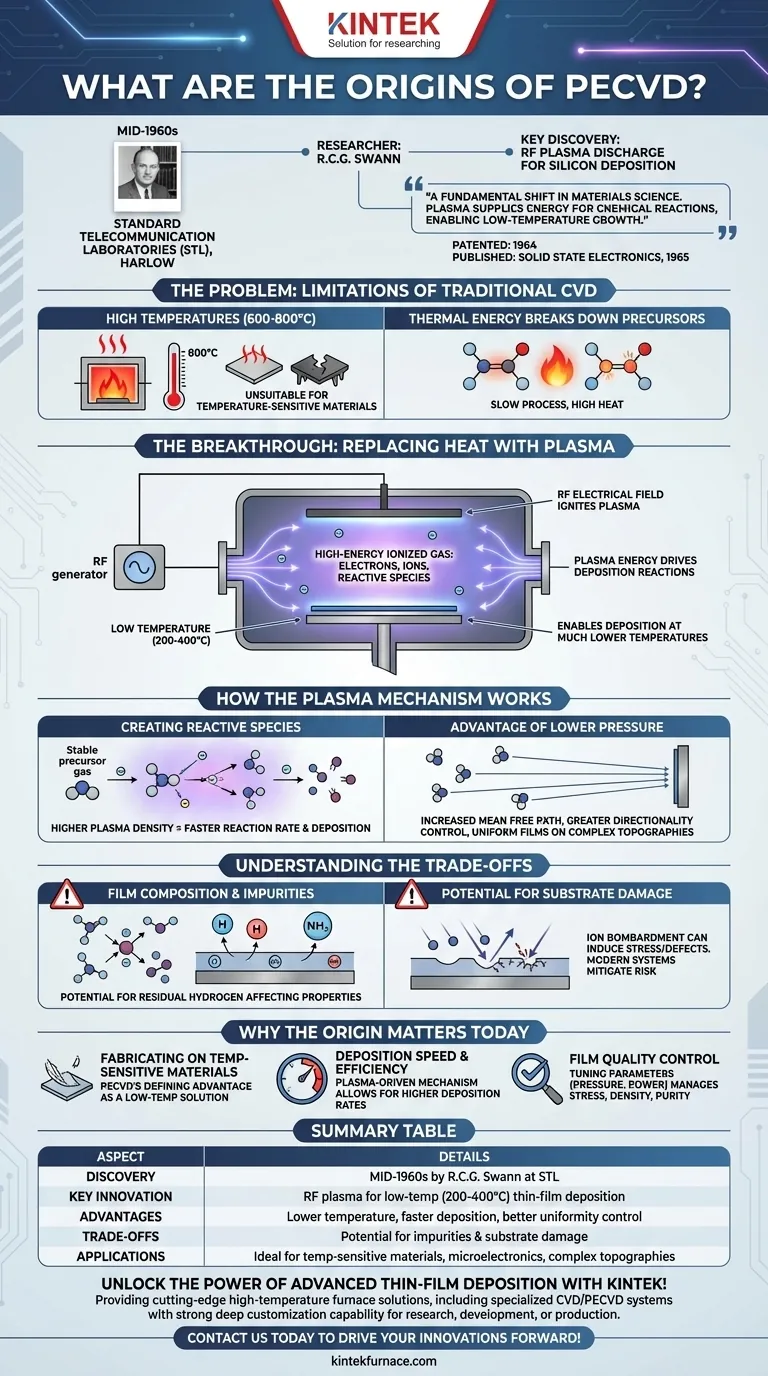
The origins of Plasma-Enhanced Chemical Vapor Deposition (PECVD) trace back to the mid-1960s at Standard Telecommunication Laboratories (STL) in Harlow, Essex. The breakthrough was made by researcher R.C.G. Swann, who discovered that using a radio frequency (RF) plasma discharge dramatically promoted the deposition of silicon compounds onto substrates. This pivotal finding was detailed in patent applications in 1964 and published in the journal Solid State Electronics in 1965.
The discovery of PECVD was a fundamental shift in materials science. It proved that a plasma could supply the energy for chemical reactions, enabling the growth of high-quality thin films at temperatures far lower than required by conventional methods.
The Problem PECVD Was Born to Solve
Limitations of Traditional CVD
Before PECVD, the primary method for depositing high-quality films was Chemical Vapor Deposition (CVD). This process relies on high temperatures, often exceeding 600-800°C, to provide the thermal energy needed to break down precursor gases and initiate chemical reactions on a substrate surface.
While effective, the high-temperature requirement of traditional CVD severely limited its applications. It was unsuitable for depositing films on substrates that could not withstand such heat, such as those with previously fabricated metal layers or temperature-sensitive materials.
The Breakthrough: Replacing Heat with Plasma
The discovery by R.C.G. Swann offered an elegant solution. Instead of relying solely on thermal energy, his method used an RF electrical field to ignite a plasma.
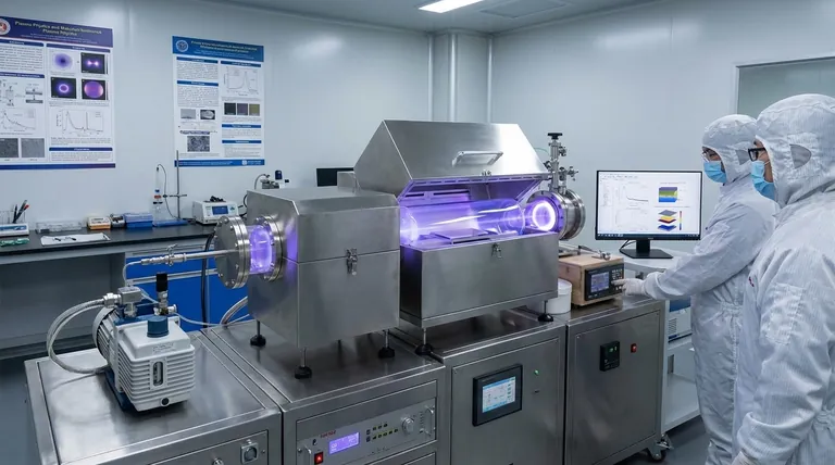
This plasma is a high-energy, ionized gas containing a dense soup of electrons, ions, and highly reactive neutral species. These energetic particles provide the activation energy needed to break chemical bonds and drive the deposition reactions, all while keeping the substrate at a much lower temperature (typically 200-400°C).
How the Plasma Mechanism Works
Creating Reactive Species
The core function of the plasma is to create a high concentration of reactive chemical species from the stable precursor gases. Increasing the plasma density directly increases the availability of these reactants.
This accelerates the overall reaction rate, allowing for faster film deposition compared to other low-temperature techniques.
The Advantage of Lower Pressure
The use of a plasma also allows the process to be run at lower pressures. This has a critical benefit: it increases the "mean free path" of gas molecules, meaning they travel further before colliding with each other.
This gives process engineers greater control over the directionality of ions moving toward the substrate. The result is a more flexible and efficient process capable of producing uniform films over complex topographies.
Understanding the Trade-offs
Film Composition and Impurities
A key trade-off in PECVD is film composition. Because the plasma reactions are so complex and energetic, precursor gases may not fully decompose.
This can lead to the incorporation of impurities, such as hydrogen from silane (SiH₄) or ammonia (NH₃) precursors, into the deposited film. This residual hydrogen can affect the film's electrical and mechanical properties.
Potential for Substrate Damage
The same energetic ions that drive the deposition reaction can also physically bombard the substrate surface. If not carefully controlled, this ion bombardment can induce stress or create defects in the underlying material.
Modern PECVD systems offer precise control over plasma power and pressure to minimize this risk, but it remains an inherent factor in the process.
Why the Origin of PECVD Still Matters Today
Understanding the foundational principle of PECVD—using plasma energy instead of thermal energy—is key to leveraging it effectively.
- If your primary focus is fabricating on temperature-sensitive materials: PECVD's origin as a low-temperature solution remains its most significant and defining advantage.
- If your primary focus is deposition speed and efficiency: The plasma-driven mechanism allows for higher deposition rates than many competing low-temperature techniques.
- If your primary focus is film quality: Understanding the plasma's role is critical for tuning parameters like pressure and power to manage film stress, density, and chemical purity.
This foundational shift from thermal to plasma-based energy fundamentally expanded the possibilities of thin-film deposition and enabled the development of modern microelectronics.
Summary Table:
| Aspect | Details |
|---|---|
| Discovery | Mid-1960s by R.C.G. Swann at Standard Telecommunication Laboratories |
| Key Innovation | Use of RF plasma for low-temperature (200-400°C) thin-film deposition |
| Advantages | Lower temperature, faster deposition, better control over film uniformity |
| Trade-offs | Potential for impurities (e.g., hydrogen) and substrate damage from ion bombardment |
| Applications | Ideal for temperature-sensitive materials, microelectronics, and complex topographies |
Unlock the Power of Advanced Thin-Film Deposition with KINTEK!
Are you working with temperature-sensitive materials or aiming for high-quality, efficient film deposition? At KINTEK, we leverage exceptional R&D and in-house manufacturing to provide cutting-edge high-temperature furnace solutions, including our specialized CVD/PECVD systems. Our strong deep customization capability ensures we can precisely meet your unique experimental requirements, whether you're in research, development, or production.
Ready to enhance your lab's capabilities? Contact us today to discuss how our PECVD systems and other furnace solutions can drive your innovations forward!
Visual Guide
Related Products
- Slide PECVD Tube Furnace with Liquid Gasifier PECVD Machine
- RF PECVD System Radio Frequency Plasma Enhanced Chemical Vapor Deposition
- Inclined Rotary Plasma Enhanced Chemical Deposition PECVD Tube Furnace Machine
- Inclined Rotary Plasma Enhanced Chemical Deposition PECVD Tube Furnace Machine
- Multi Heating Zones CVD Tube Furnace Machine for Chemical Vapor Deposition Equipment
People Also Ask
- What plasma source is used in PE-CVD tube furnaces? Unlock Low-Temperature, High-Quality Deposition
- How does PECVD equipment contribute to TOPCon bottom cells? Mastering Hydrogenation for Maximum Solar Efficiency
- What are the advantages of using a tube furnace CVD system for Cu(111)/graphene? Superior Scalability and Quality
- What are the disadvantages of tube furnace cracking when processing heavy raw materials? Avoid Costly Downtime and Inefficiency
- What is plasma in the context of PECVD? Unlock Low-Temperature Thin Film Deposition


