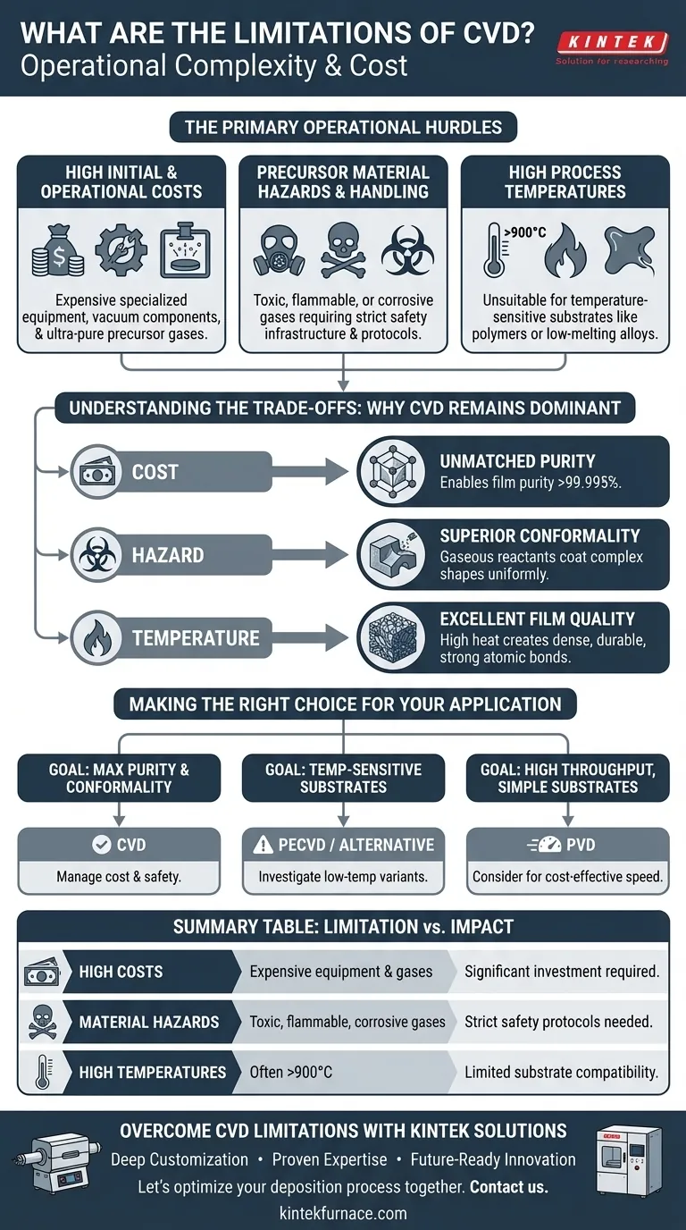
At its core, the limitations of Chemical Vapor Deposition (CVD) revolve around operational complexity and cost. While it produces exceptionally high-quality films, the process demands significant investment in equipment, involves potentially hazardous materials that require strict safety protocols, and often operates at very high temperatures that can limit the types of materials you can coat.
CVD is a powerful and versatile deposition technique, but its primary limitations are not in the quality of the end product. Instead, the challenges lie in the high capital and operational costs, stringent safety requirements for handling precursor gases, and the high processing temperatures inherent to many of its forms.
The Primary Operational Hurdles of CVD
To properly evaluate CVD, you must look beyond the finished coating and consider the practical realities of running the process. These operational factors are often the deciding criteria when comparing it to other methods like Physical Vapor Deposition (PVD).
High Initial and Operational Costs
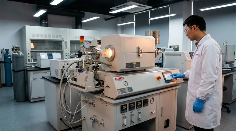
The financial barrier to entry for CVD can be substantial. The reaction chambers, gas delivery systems, and vacuum components are specialized and expensive.
Furthermore, the precursor gases—the chemical building blocks for the film—are often highly pure, which makes them costly to produce and procure. This contrasts with some PVD methods that may use a solid, more affordable target material.
Precursor Material Hazards and Handling
Safety is a non-negotiable and complex aspect of any CVD operation. The precursor gases are frequently toxic, flammable, or corrosive.
This necessitates a significant investment in safety infrastructure. This includes specialized gas cabinets, leak detectors, abatement systems to treat exhaust gas, and rigorous training protocols for all personnel. These safety measures add layers of cost and complexity to the facility and process.
High Process Temperatures
Traditional thermal CVD processes often require extremely high temperatures, sometimes exceeding 900°C, to drive the necessary chemical reactions.
This high heat level makes it unsuitable for coating temperature-sensitive substrates like polymers or certain low-melting-point alloys. While variants like Plasma-Enhanced CVD (PECVD) were developed to operate at lower temperatures, the limitation remains a primary consideration for conventional CVD.
Understanding the Trade-offs: Why CVD is Still a Dominant Process
The limitations of CVD are significant, but they are the necessary trade-offs for achieving results that are difficult or impossible with other methods. Understanding this balance is key to making an informed decision.
Limitation vs. Benefit: Cost for Unmatched Purity
The high cost of equipment and ultra-pure precursors directly enables one of CVD's greatest strengths: exceptional film purity. Films produced by CVD can exceed 99.995% purity, which is critical for high-performance applications in semiconductors and aerospace.
Limitation vs. Benefit: Hazard for Superior Conformality
The use of gaseous reactants, despite their hazards, is what allows CVD to create perfectly conformal coatings. The gas can penetrate and coat complex, three-dimensional shapes and internal surfaces with outstanding uniformity. This is a distinct advantage over line-of-sight processes like PVD.
Limitation vs. Benefit: Temperature for Excellent Film Quality
For thermal CVD, the high process temperatures are not just a drawback; they are often essential for creating highly dense, crystalline, and durable films. The thermal energy promotes the formation of strong atomic bonds, resulting in coatings with superior mechanical and chemical properties.
Making the Right Choice for Your Application
Choosing a deposition method requires aligning your primary goal with the inherent strengths and weaknesses of the process.
- If your primary focus is maximum film purity and conformal coverage on complex parts: CVD is often the superior choice, provided you can manage the significant investment in cost and safety infrastructure.
- If your primary focus is coating temperature-sensitive substrates like polymers: You must specifically investigate low-temperature variants like PECVD or consider alternative technologies altogether.
- If your primary focus is high throughput on simple, flat substrates: A process like PVD may offer a more cost-effective and faster solution, as the unique advantages of CVD may not be necessary.
Ultimately, understanding the limitations of CVD is the first step toward strategically leveraging its powerful capabilities for the right application.
Summary Table:
| Limitation | Key Challenge | Impact on Application |
|---|---|---|
| High Costs | Expensive equipment and ultra-pure precursor gases | Significant capital and operational investment required |
| Material Hazards | Toxic, flammable, or corrosive gases | Need for strict safety protocols and infrastructure |
| High Temperatures | Often exceeds 900°C, limiting substrate compatibility | Unsuitable for temperature-sensitive materials like polymers |
Ready to Overcome CVD Limitations with Precision-Engineered Solutions?
At KINTEK, we understand that navigating the challenges of Chemical Vapor Deposition requires more than just equipment—it demands expertise and customization. Our advanced high-temperature furnace solutions, including Tube Furnaces, Vacuum & Atmosphere Furnaces, and specialized CVD/PECVD Systems, are designed to address the very limitations discussed here.
Why Choose KINTEK?
- Deep Customization: We tailor our systems to your specific research needs, whether you require precise temperature control, enhanced safety features, or compatibility with unique substrates.
- Proven Expertise: Leveraging our exceptional R&D and in-house manufacturing capabilities, we deliver reliable, high-performance solutions for diverse laboratories.
- Future-Ready Innovation: From Muffle and Rotary Furnaces to cutting-edge CVD systems, our product line evolves with your challenges in mind.
Let’s optimize your deposition process together. Contact us today to discuss how KINTEK can empower your research with safer, more efficient, and cost-effective solutions!
Visual Guide
Related Products
- Custom Made Versatile CVD Tube Furnace Chemical Vapor Deposition CVD Equipment Machine
- Multi Heating Zones CVD Tube Furnace Machine for Chemical Vapor Deposition Equipment
- HFCVD Machine System Equipment for Drawing Die Nano Diamond Coating
- Split Chamber CVD Tube Furnace with Vacuum Station CVD Machine
- 915MHz MPCVD Diamond Machine Microwave Plasma Chemical Vapor Deposition System Reactor
People Also Ask
- What are the practical applications of gate media prepared by CVD tube furnaces? Unlock Advanced Electronics and More
- How does CVD tube furnace sintering enhance graphene growth? Achieve Superior Crystallinity and High Electron Mobility
- How might AI and machine learning enhance CVD tube furnace processes? Boost Quality, Speed, and Safety
- What are the benefits of developing new precursor materials for CVD tube furnaces? Unlock Advanced Thin-Film Synthesis
- What is the working principle of a CVD tube furnace? Achieve Precise Thin Film Deposition for Your Lab


