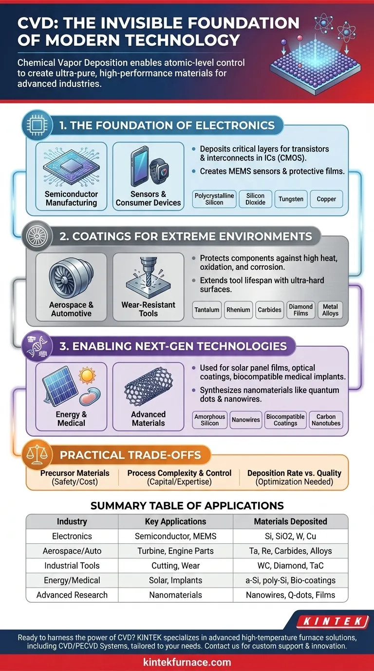
In short, materials deposited by Chemical Vapor Deposition (CVD) are foundational to virtually every modern high-technology industry. From the microprocessors in our smartphones to the protective coatings on jet engine turbines, CVD is used to create ultra-pure, high-performance thin films and materials that are otherwise impossible to manufacture. Its applications span electronics, aerospace, automotive, and next-generation energy and medical technologies.
The true value of CVD lies not just in a single application, but in its profound versatility. It is a process that gives engineers atomic-level control to deposit a vast range of materials—including metals, ceramics, and semiconductors—onto substrates, enabling the precise material properties required for advanced manufacturing.
The Foundation of Modern Electronics
The electronics industry is arguably the largest and most critical user of CVD. The process's ability to deposit exceptionally pure and uniform thin films is essential for creating the microscopic structures that power our digital world.
Semiconductor Manufacturing
At the heart of every computer, smartphone, and data center are integrated circuits built on silicon wafers. CVD is the workhorse process used to deposit the critical layers of material that form transistors and interconnects.
This includes depositing polycrystalline silicon for transistor gates, silicon dioxide as an insulator, and metals like tungsten and copper to wire the millions of components on a single chip. Without CVD, modern CMOS (Complementary Metal-Oxide-Semiconductor) technology would not exist.
Advanced Sensors and Consumer Devices
Beyond core processing, CVD is used to create specialized components. It enables the fabrication of sensors for automotive systems, smart home devices, and HVAC controls.
In consumer electronics like wearables and "hearables," CVD provides the thin films needed for everything from MEMS (Micro-Electro-Mechanical Systems) microphones to protective, moisture-resistant barriers on internal components.
High-Performance Coatings for Extreme Environments
Many industries rely on materials that can withstand extreme temperatures, corrosive chemicals, and intense mechanical wear. CVD provides a way to apply ultra-hard and resilient coatings to less durable base materials.
Aerospace and Automotive Components
CVD is used to deposit advanced metal alloys and ceramic coatings on components like turbine blades and engine parts. These layers protect against high-temperature oxidation and corrosion, extending component life and improving safety and fuel efficiency.
Materials like tantalum, rhenium, and specialized carbides are deposited to create thermal barriers and wear-resistant surfaces that are critical for performance in these demanding sectors.
Wear-Resistant and Cutting Tools
The exceptional hardness of certain materials makes them ideal for industrial tools. CVD is used to coat machine tools, drills, and cutting blades with materials like tungsten carbide, tantalum carbide, and even diamond films.
These coatings dramatically increase the tool's lifespan, reduce friction, and allow for higher-speed, more precise machining operations.
Enabling Next-Generation Technologies
CVD is not just a process for refining existing technologies; it is a key enabler for creating entirely new ones. Its precision allows researchers to build materials from the atom up.
Energy, Optics, and Medical Devices
In the energy sector, CVD is used to create the amorphous and polycrystalline silicon thin films that form the basis of many solar panels. For optics, it's used to deposit anti-reflective coatings on lenses and create specialized optical films.
The process is also being leveraged to create biocompatible coatings for medical implants and to produce materials for advanced medical imaging.
Advanced Materials and Structures
Looking toward the future, CVD is a primary method for synthesizing advanced materials with unique properties. This includes growing complex structures like carbon nanotubes and nanowires.
It is also used to create quantum dots and other nanomaterials that are central to research in next-generation computing, displays, and biosensors.
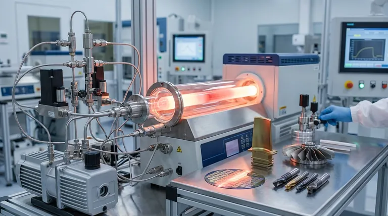
Understanding the Practical Trade-offs
While incredibly powerful, CVD is a complex and resource-intensive process. Its application is not without significant practical considerations that dictate its use.
The Role of Precursor Materials
CVD works by introducing reactive precursor gases into a chamber. The availability, cost, purity, and safety of these precursors are major factors. Many are highly toxic, flammable, or corrosive, requiring extensive safety and handling infrastructure.
Process Complexity and Control
Achieving a high-quality, uniform film requires precise control over numerous variables, including temperature, pressure, gas flow rates, and chamber chemistry. CVD systems are sophisticated pieces of equipment that demand significant capital investment and operational expertise.
Deposition Rate vs. Quality
There is often a direct trade-off between the speed of deposition and the quality of the resulting film. Faster deposition rates can sometimes introduce defects or impurities, so processes must be carefully optimized for the specific quality requirements of the application.
Making the Right Choice for Your Goal
Deciding if CVD is the appropriate process depends entirely on the material properties you need to achieve.
- If your primary focus is high-volume electronics manufacturing: CVD is the non-negotiable standard for creating the ultra-pure, uniform semiconductor and dielectric thin films required for integrated circuits.
- If your primary focus is mechanical performance and durability: CVD is the leading choice for applying exceptionally hard, wear-resistant, and thermally stable coatings like diamond or tungsten carbide.
- If your primary focus is research and advanced materials: CVD offers unparalleled flexibility for synthesizing novel material structures like nanotubes, nanowires, and custom thin films for experimental applications.
Ultimately, Chemical Vapor Deposition is the invisible but essential process that engineers the fundamental materials of our modern technological landscape.
Summary Table:
| Industry | Key CVD Applications | Materials Deposited |
|---|---|---|
| Electronics | Semiconductor manufacturing, sensors, MEMS devices | Polycrystalline silicon, silicon dioxide, tungsten, copper |
| Aerospace & Automotive | Turbine blade coatings, engine parts protection | Tantalum, rhenium, carbides, metal alloys |
| Industrial Tools | Cutting tools, wear-resistant coatings | Tungsten carbide, diamond films, tantalum carbide |
| Energy & Medical | Solar panels, optical coatings, medical implants | Amorphous silicon, polycrystalline silicon, biocompatible coatings |
| Advanced Research | Nanomaterials, quantum dots, carbon nanotubes | Nanowires, quantum dots, custom thin films |
Ready to harness the power of CVD for your laboratory? At KINTEK, we specialize in delivering advanced high-temperature furnace solutions tailored to your unique needs. Leveraging our exceptional R&D and in-house manufacturing, we offer a comprehensive product line—including Muffle, Tube, Rotary Furnaces, Vacuum & Atmosphere Furnaces, and CVD/PECVD Systems—supported by deep customization capabilities. Whether you're in electronics, aerospace, energy, or research, our expertise ensures precise material deposition for superior performance and innovation. Contact us today to discuss how we can elevate your projects with cutting-edge technology and customized support!
Visual Guide
Related Products
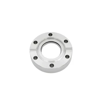
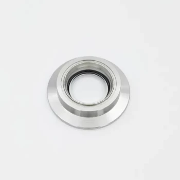
- HFCVD Machine System Equipment for Drawing Die Nano Diamond Coating
- Custom Made Versatile CVD Tube Furnace Chemical Vapor Deposition CVD Equipment Machine
- 915MHz MPCVD Diamond Machine Microwave Plasma Chemical Vapor Deposition System Reactor
- Multi Heating Zones CVD Tube Furnace Machine for Chemical Vapor Deposition Equipment
- MPCVD Machine System Reactor Bell-jar Resonator for Lab and Diamond Growth
People Also Ask
- How can customers maximize the quality of CVD coatings? Master Pre-Coating Prep for Superior Results
- What role does Chemical Vapor Deposition (CVD) equipment play in the surface coating of carbon fibers for composites?
- What is the advantage of using a CVD system for coating turbine blades? Master Complex Geometries with Ease
- What is the significance of the vacuum pressure control system in the CVD coating process for powders?
- What materials are commonly used in CVD coating systems? Explore Key Materials for Superior Coatings