While a foundational technique, traditional chemical vapor deposition (CVD) presents significant obstacles for the practical use of 2D materials. Its primary disadvantages are the extremely high operating temperatures, a dependency on metal catalysts, and the destructive post-growth transfer process required to move the material. These issues introduce contamination and defects that compromise the final material's quality and limit its application in modern electronics.
The core problem with traditional CVD is not just one of inconvenience, but of fundamental conflict. It uses a harsh, high-temperature process to create high-quality 2D materials, only to require a subsequent transfer step that inevitably contaminates and damages them, undermining the very quality it sought to achieve.
The Challenge of High-Temperature Growth
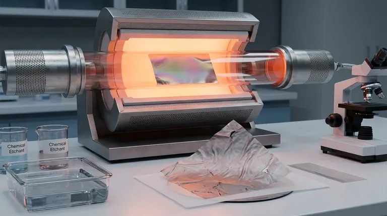
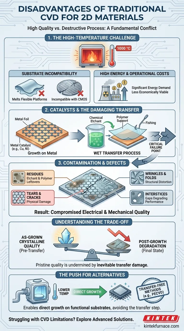
The conditions required for traditional CVD are often its biggest liability. The process typically operates at temperatures around 1000 °C, creating a cascade of limitations.
Thermal Budget and Substrate Incompatibility
Such extreme heat is incompatible with most substrates used in device fabrication. It prevents the direct growth of 2D materials onto silicon CMOS wafers, flexible polymers, or other temperature-sensitive platforms.
This incompatibility forces a multi-step manufacturing process, adding complexity and cost while preventing seamless integration with existing semiconductor technologies.
Energy and Operational Costs
Sustaining temperatures of 1000 °C requires a significant amount of energy. For large-scale production, these energy demands translate directly into higher operational costs, making the process less economically viable compared to lower-temperature alternatives.
The Problem with Catalysts and Transfer
Beyond temperature, the mechanics of traditional CVD introduce unavoidable points of failure. The process relies on a catalyst, which necessitates a damaging transfer step.
Dependence on Metal Catalysts
Traditional CVD typically uses a metal foil, such as copper or nickel, as a catalytic substrate. The 2D material—for example, graphene—grows on the surface of this metal.
While effective for growth, this means the material is not on its final target substrate. It must be moved.
The Inevitable, Damaging Transfer Step
This is the most critical point of failure. To move the 2D film, the underlying metal catalyst is typically dissolved with chemical etchants. A polymer support layer (like PMMA) is used to handle the fragile film during this process.
The film is then "fished" out of the solution and placed onto the final substrate, after which the polymer support layer is dissolved.
Sources of Contamination and Defects
This wet transfer process is notoriously "dirty" and destructive. It is a primary source of contamination from etchant and polymer residues that are nearly impossible to fully remove.
Furthermore, the physical handling introduces defects like tears, wrinkles, and folds. The gaps and voids left by this process, known as interstices, severely degrade the material's electrical and mechanical performance. The final film is often a patchwork of high-quality domains and damaged, contaminated regions.
Understanding the Trade-offs
Despite these severe drawbacks, traditional CVD is not without its merits. Understanding its core trade-off is key to making an informed decision.
The Advantage: As-Grown Crystalline Quality
The primary reason for using traditional thermal CVD is its ability to produce large-area films with high crystallinity before the transfer step. The high temperature provides the energy needed for atoms to arrange into a near-perfect lattice on the catalyst surface.
The Consequence: Post-Growth Degradation
The trade-off is that the pristine, as-grown quality is almost immediately compromised. The benefits of high crystallinity are undermined by the contamination and structural damage introduced during transfer. For device applications, the performance is dictated by the final, post-transfer state of the material, not its ideal as-grown state.
The Push Toward Transfer-Free Methods
These disadvantages have driven significant research into alternatives like Plasma-Enhanced CVD (PECVD). Such methods operate at much lower temperatures and enable the direct, transfer-free growth of 2D materials onto non-catalytic insulating substrates. This approach avoids the transfer step entirely, preserving the material's integrity.
Making the Right Choice for Your Application
Selecting a synthesis method requires matching the process capabilities to your end goal. The drawbacks of traditional CVD make it well-suited for some tasks but entirely inappropriate for others.
- If your primary focus is fundamental research on material properties: Traditional CVD is excellent for producing highly crystalline films on a catalyst foil for analysis before any transfer is attempted.
- If your primary focus is scalable device manufacturing: The contamination, defects, and low-throughput nature of the transfer process make traditional CVD a poor choice for industrial-scale electronics.
- If your primary focus is integration with flexible or CMOS electronics: The high process temperature of traditional CVD makes it completely unsuitable, and low-temperature, direct-growth methods are necessary.
Understanding these inherent limitations is the first step toward selecting a synthesis method that delivers the performance your application truly requires.
Summary Table:
| Disadvantage | Impact on 2D Materials |
|---|---|
| High operating temperatures (~1000°C) | Incompatible with temperature-sensitive substrates, increases energy costs |
| Dependence on metal catalysts | Requires post-growth transfer, leading to contamination and defects |
| Destructive transfer process | Introduces tears, wrinkles, and residues, degrading electrical and mechanical performance |
Struggling with the limitations of traditional CVD for your 2D material applications? At KINTEK, we specialize in advanced high-temperature furnace solutions, including CVD and PECVD systems, to help you overcome these challenges. Leveraging our exceptional R&D and in-house manufacturing, we offer deep customization to precisely meet your unique experimental needs—whether you're in research, scalable device manufacturing, or integrating with flexible or CMOS electronics. Our product line, featuring Muffle, Tube, Rotary Furnaces, Vacuum & Atmosphere Furnaces, and CVD/PECVD Systems, ensures superior performance and efficiency. Contact us today to discuss how we can enhance your lab's capabilities and achieve better results with tailored solutions!
Visual Guide
Related Products
- HFCVD Machine System Equipment for Drawing Die Nano Diamond Coating
- Cylindrical Resonator MPCVD Machine System for Lab Diamond Growth
- 915MHz MPCVD Diamond Machine Microwave Plasma Chemical Vapor Deposition System Reactor
- MPCVD Machine System Reactor Bell-jar Resonator for Lab and Diamond Growth
- Custom Made Versatile CVD Tube Furnace Chemical Vapor Deposition CVD Equipment Machine
People Also Ask
- What is the function of high-purity Argon (Ar) gas during CVD? Optimize Your Thin Film Uniformity and Purity
- What is the significance of the vacuum pressure control system in the CVD coating process for powders?
- What role does Chemical Vapor Deposition (CVD) equipment play in the surface coating of carbon fibers for composites?
- What materials are commonly used in CVD coating systems? Explore Key Materials for Superior Coatings
- What core function does CVD equipment serve in h-BN anti-corrosion? Master Precision Synthesis for High-Performance Films


