Historically, the most common and foundational use of aluminum films in semiconductor devices is to create the electrical interconnects, or "wiring," that connect the millions or billions of transistors on a chip. These thin metal pathways are responsible for distributing power and transmitting data signals, forming the fundamental circulatory system of the integrated circuit.
While once the default choice for all on-chip wiring, aluminum's role has evolved. Its story reveals a core engineering trade-off between manufacturing simplicity and the physical limits of materials at the nanoscale.
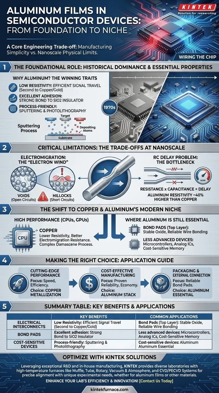
The Foundational Role of Aluminum as an Interconnect
For decades, aluminum was the undisputed material of choice for metallization in semiconductor fabrication. This was not by accident; it possesses a unique combination of properties that made it nearly perfect for the task in the early eras of chip manufacturing.
Why Aluminum? The Essential Properties
Aluminum offers low electrical resistivity, second only to more complex metals like copper and gold. This ensures that electrical signals can travel through the chip's wiring with minimal loss and delay.
Crucially, it also demonstrates excellent adhesion to silicon dioxide (SiO2), which is the primary insulating material used to separate the different layers of wiring. This strong bond prevents the metal layers from peeling or delaminating during manufacturing or operation.
A Process-Friendly Material
Fabricating circuits with aluminum is a relatively straightforward and well-understood process. It can be easily deposited in thin, uniform films using a technique called sputtering.
Once deposited, these films can be precisely patterned into wires using photolithography and dry etching, allowing for the creation of incredibly complex circuit layouts.
Understanding the Trade-offs: Critical Limitations
As transistors shrank and clock speeds increased, the inherent physical limitations of aluminum became critical roadblocks to further performance gains, leading to significant reliability challenges.
The Primary Failure: Electromigration
The most significant weakness of aluminum is its susceptibility to electromigration. At the high current densities found in modern chips, the flow of electrons can physically push aluminum atoms along the wire.
This "electron wind" gradually creates voids (gaps) in some areas and hillocks (pile-ups) in others. A large enough void will cause an open circuit, while a hillock can create a short circuit to an adjacent wire, both resulting in chip failure.
The RC Delay Problem
As interconnects become thinner and more densely packed, their resistance (R) and the capacitance (C) between them increase. The product of these two values, the RC delay, dictates how quickly a signal can travel.
Aluminum's resistivity, while low, is about 40% higher than that of copper. This higher resistance became a primary bottleneck, limiting the maximum speed at which a chip could operate.
The Shift to Copper and Aluminum's Modern Niche
These limitations forced the industry to transition to copper for high-performance interconnects, a major technological shift that began in the late 1990s.
Copper's Ascendancy in High Performance
Copper has lower resistivity and significantly better resistance to electromigration. However, it is much more difficult to process and requires barrier layers to prevent it from diffusing into and poisoning the silicon. This led to the development of the complex Damascene process.
Where Aluminum Is Still Essential
Despite the shift to copper for the finest layers of wiring in CPUs and GPUs, aluminum has not disappeared. It remains the material of choice in several key areas.
Its most prominent modern use is for the thick, top-level metal layers and bond pads. These are the connection points where the chip is physically wired to the package. Aluminum forms a stable, self-passivating oxide layer that is ideal for reliable wire bonding. It is also still widely used in less advanced or more cost-sensitive devices like microcontrollers, analog ICs, and some memory and power semiconductor devices.
Making the Right Choice for Your Application
The choice between aluminum and copper is dictated entirely by the performance requirements, cost constraints, and specific function within the device.
- If your primary focus is cutting-edge performance (CPUs, GPUs): Copper metallization is the non-negotiable standard for performance-critical interconnects due to its superior conductivity.
- If your primary focus is cost-effective manufacturing for less demanding chips (microcontrollers, analog): Aluminum remains a proven, reliable, and economical choice for the entire interconnect stack.
- If your primary focus is packaging and external connection: Aluminum is the essential material for top-level bond pads across nearly all chip types to ensure a reliable connection to the outside world.
Understanding the historic role and modern niche of aluminum provides a clear perspective on the material science trade-offs that continue to drive semiconductor innovation.
Summary Table:
| Use Case | Key Benefits | Common Applications |
|---|---|---|
| Electrical Interconnects | Low resistivity, excellent adhesion to SiO2, process-friendly | Early chips, microcontrollers, analog ICs |
| Bond Pads | Stable oxide layer, reliable for wire bonding | Top-level connections in nearly all chip types |
| Cost-Sensitive Devices | Economical, proven reliability | Less advanced ICs, power semiconductors |
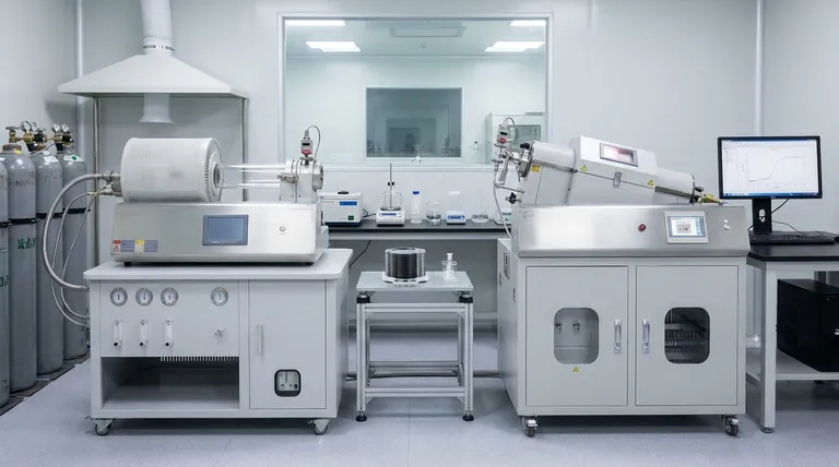
Optimize your semiconductor processes with KINTEK's advanced furnace solutions! Leveraging exceptional R&D and in-house manufacturing, we provide diverse laboratories with high-temperature furnaces like Muffle, Tube, Rotary, Vacuum & Atmosphere, and CVD/PECVD Systems. Our strong deep customization capability ensures precise alignment with your unique experimental needs, whether for developing aluminum films or other materials. Contact us today to enhance your lab's efficiency and innovation!
Visual Guide
Related Products
- Custom Made Versatile CVD Tube Furnace Chemical Vapor Deposition CVD Equipment Machine
- Multi Heating Zones CVD Tube Furnace Machine for Chemical Vapor Deposition Equipment
- 915MHz MPCVD Diamond Machine Microwave Plasma Chemical Vapor Deposition System Reactor
- Slide PECVD Tube Furnace with Liquid Gasifier PECVD Machine
- Ultra High Vacuum CF Observation Window Flange with High Borosilicate Glass Sight Glass
People Also Ask
- What improvements can be made to the bonding force of gate dielectric films using a CVD tube furnace? Enhance Adhesion for Reliable Devices
- What is a CVD tube furnace and what is its primary function? Discover Precision Thin-Film Deposition
- What are the practical applications of gate media prepared by CVD tube furnaces? Unlock Advanced Electronics and More
- What temperature range do standard CVD tube furnaces operate at? Unlock Precision for Your Material Deposition
- What customization options are available for CVD tube furnaces? Tailor Your System for Superior Material Synthesis