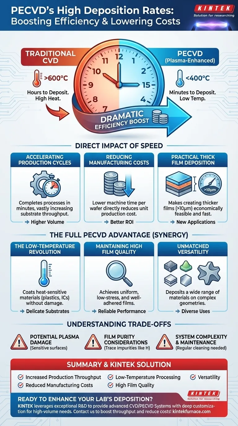
At its core, the primary benefit of Plasma-Enhanced Chemical Vapor Deposition (PECVD) and its high deposition rates is a dramatic increase in manufacturing efficiency. This speed allows for the creation of thin films in minutes instead of hours, which directly translates to higher production throughput and significantly lower costs per unit, making it a cornerstone of modern high-volume manufacturing.
The true value of PECVD's speed is not just the rate itself, but its ability to achieve this speed at low temperatures. This unique combination unlocks the ability to coat heat-sensitive materials without sacrificing the economic viability required for mass production.
The Direct Impact of High Deposition Rates
The speed of PECVD is not just an incremental improvement; it fundamentally changes the economics and capabilities of thin-film deposition.
Accelerating Production Cycles
A traditional Chemical Vapor Deposition (CVD) process might take hours to deposit a specific film thickness. PECVD, by using plasma to energize the precursor gases, accelerates these chemical reactions dramatically.
This allows the same process to be completed in a matter of minutes, vastly increasing the number of substrates that can be processed in a given period.
Reducing Manufacturing Costs
In any manufacturing environment, machine time is a direct cost. By reducing the time required to process each wafer or part, PECVD lowers the overall cost of production.
This cost-effectiveness is a key reason why PECVD is so widely adopted in industries like semiconductor fabrication and solar panel manufacturing, where volume and cost-per-unit are critical metrics.
Enabling Practical Thick Film Deposition
While often used for "thin" films, some applications require thicker coatings, potentially greater than 10 micrometers (μm).
PECVD's high deposition rate makes the creation of these thicker films practical from a time and cost perspective, a task that would be prohibitively slow and expensive using many conventional, lower-rate CVD methods.
Why Speed Isn't the Whole Story: The Full PECVD Advantage
The high deposition rate is a powerful feature, but its true impact is realized when combined with the other inherent advantages of the PECVD process.
The Low-Temperature Revolution
Perhaps the most significant benefit of PECVD is its low processing temperature, often below 400°C. Traditional CVD requires very high temperatures (often >600°C) to drive the necessary chemical reactions.
This low-temperature capability, combined with high speed, allows for the deposition of high-quality films on temperature-sensitive materials like plastics, polymers, and fully-processed integrated circuits that would be damaged or destroyed by high-heat methods.
Maintaining High Film Quality
Despite the high speed, PECVD does not inherently sacrifice quality. The plasma-enhanced process can produce films that are highly uniform across large-area substrates.
Furthermore, these films typically exhibit low internal stress and good adhesion to the substrate, making them robust and resistant to cracking or delamination. The process also allows for excellent control over material properties like refractive index and hardness.
Unmatched Versatility
PECVD is a highly versatile technology capable of depositing a wide range of materials, including dielectrics (like silicon nitride and silicon dioxide), semiconductors, and even some metals.
Its ability to conformally coat complex, non-planar geometries makes it valuable for a diverse set of applications, from microelectronics to protective coatings on industrial parts. The high deposition rate makes applying these varied materials economically feasible.
Understanding the Trade-offs
While powerful, PECVD is not a universal solution. Understanding its limitations is key to making an informed decision.
Potential for Plasma-Induced Damage
The high-energy plasma that enables low-temperature, high-rate deposition can sometimes cause surface damage to highly sensitive substrates if the process is not precisely controlled.
Film Purity Considerations
For certain highly specialized applications requiring the absolute highest material purity (e.g., specific epitaxial layers), slower, higher-temperature processes like Low-Pressure CVD (LPCVD) may still be preferred. PECVD films can sometimes contain trace impurities, such as hydrogen, from the precursor gases.
System Complexity and Maintenance
PECVD systems are more complex than some simple thermal CVD reactors. The plasma generation hardware requires careful maintenance, and chamber cleaning is a regular necessity to remove polymer byproducts that can form during deposition.
Making the Right Choice for Your Goal
Selecting a deposition method depends entirely on your project's primary objective.
- If your primary focus is maximum throughput and cost efficiency: PECVD is an exceptional choice, especially for high-volume manufacturing where its speed provides a decisive economic advantage.
- If your primary focus is coating heat-sensitive substrates: PECVD is often the only viable option, as its low-temperature nature protects delicate materials while still offering production-worthy speed.
- If your primary focus is the absolute highest film purity: You may need to consider slower, higher-temperature methods, accepting the trade-off in speed and substrate limitation for superior material quality.
Ultimately, PECVD's high deposition rate is the engine that makes its unique combination of low-temperature processing and high-quality film deposition a dominant and enabling technology in modern manufacturing.
Summary Table:
| Benefit | Description |
|---|---|
| Increased Production Throughput | High deposition rates allow thin films to be created in minutes, not hours, boosting output. |
| Reduced Manufacturing Costs | Faster processing lowers machine time and cost per unit, ideal for high-volume industries. |
| Low-Temperature Processing | Enables coating of heat-sensitive materials like plastics without damage, combined with speed. |
| High Film Quality | Maintains uniformity, low stress, and good adhesion even at high deposition rates. |
| Versatility | Deposits various materials (e.g., dielectrics, semiconductors) on complex geometries efficiently. |
Ready to enhance your lab's thin-film deposition with high-efficiency solutions? KINTEK leverages exceptional R&D and in-house manufacturing to provide advanced high-temperature furnace solutions, including CVD/PECVD Systems. Our strong deep customization capability ensures we precisely meet your unique experimental needs, whether you're in semiconductor fabrication, solar panel manufacturing, or other high-volume industries. Contact us today to discuss how our tailored PECVD systems can boost your production throughput and reduce costs!
Visual Guide
Related Products
- Slide PECVD Tube Furnace with Liquid Gasifier PECVD Machine
- RF PECVD System Radio Frequency Plasma Enhanced Chemical Vapor Deposition
- Inclined Rotary Plasma Enhanced Chemical Deposition PECVD Tube Furnace Machine
- Inclined Rotary Plasma Enhanced Chemical Deposition PECVD Tube Furnace Machine
- Multi Heating Zones CVD Tube Furnace Machine for Chemical Vapor Deposition Equipment
People Also Ask
- What plasma source is used in PE-CVD tube furnaces? Unlock Low-Temperature, High-Quality Deposition
- What are the main advantages of PECVD tube furnaces compared to CVD tube furnaces? Lower Temp, Faster Deposition, and More
- What role does a Tube Furnace play in the CVD growth of carbon nanotubes? Achieve High-Purity CNT Synthesis
- How does PECVD equipment contribute to TOPCon bottom cells? Mastering Hydrogenation for Maximum Solar Efficiency
- How does a hydrogen reduction environment in an industrial tube furnace facilitate gold-copper alloy microspheres?


