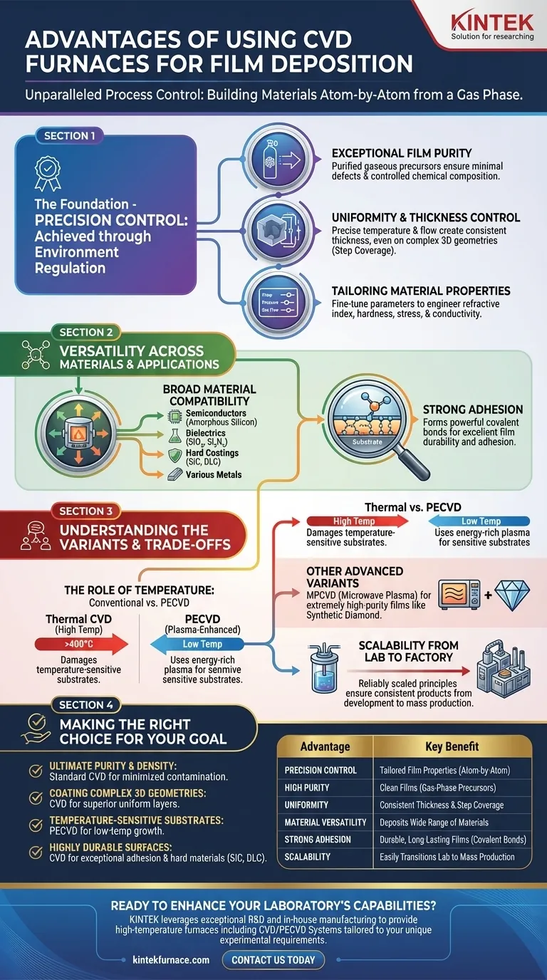
At their core, the advantages of using a Chemical Vapor Deposition (CVD) furnace stem from a single principle: unparalleled process control. By reacting purified gases directly on a substrate surface, CVD enables the creation of exceptionally high-quality thin films with precisely engineered properties, uniformity, and purity that are difficult to achieve with other methods.
The fundamental strength of a CVD furnace is its ability to build materials atom-by-atom from a gas phase. This gives you precise control over the final film's purity, structure, and physical properties in a way that liquid or solid-based deposition techniques cannot match.
The Foundation of CVD: Precision Control
The defining feature of CVD is the level of control it offers over the deposition environment. This control directly translates into superior film quality.
Achieving Exceptional Film Purity
Because the entire process begins with gaseous reactants, or precursors, they can be purified to extremely high levels before entering the reaction chamber.
This gas-phase reaction inherently avoids the introduction of contaminants often found in sputtering targets or evaporation sources, resulting in films with minimal defects and a highly controlled chemical composition.
Ensuring Uniformity and Thickness Control
CVD furnaces are engineered for precise temperature regulation and optimized gas flow dynamics across the substrate surface.
This ensures the chemical reaction occurs at a consistent rate everywhere, producing a film with exceptional uniformity in thickness. This is true even across large wafers or components with complex, three-dimensional geometries, a feature known as good step coverage.
Tailoring Material Properties
The final properties of the deposited film are a direct result of the process conditions.
By finely tuning parameters like temperature, pressure, gas mixture, and flow rates, you can engineer specific material characteristics. This includes refractive index, material stress, hardness, and electrical conductivity.
Versatility Across Materials and Applications
CVD is not a single technique but a family of technologies adaptable to a vast range of materials and substrate requirements.
Broad Material Compatibility
One of the most significant advantages is its material versatility. The CVD process can be adapted to deposit a wide array of materials.
This includes semiconductors like amorphous silicon, dielectrics like silicon oxide (SiO₂) and silicon nitride (Si₃N₄), hard coatings like silicon carbide (SiC) and diamond-like carbon (DLC), and various metals.
Strong Adhesion to Substrates
The "chemical" aspect of CVD creates a powerful bond between the deposited film and the substrate.
Unlike some physical deposition methods where the film is simply layered on top, CVD forms strong covalent bonds at the interface. This results in excellent film adhesion and durability.
Understanding the Variants and Trade-offs
While powerful, it's crucial to understand the different types of CVD and their specific applications to make an informed decision. Not all CVD processes are the same.
The Role of Temperature: Conventional vs. PECVD
Conventional thermal CVD often requires high temperatures to drive the chemical reaction, which can damage temperature-sensitive substrates like polymers or pre-processed semiconductor wafers.
To solve this, variants like Plasma-Enhanced CVD (PECVD) were developed. PECVD uses an energy-rich plasma to facilitate the reaction, allowing for high-quality film deposition at much lower temperatures, often below 400°C.
Other Advanced Variants
Other specialized techniques like Microwave Plasma CVD (MPCVD) exist to produce extremely high-purity films, such as synthetic diamond, offering another layer of process control for demanding research and industrial applications.
Scalability from Lab to Factory
A key industrial advantage is scalability. The principles governing the CVD process are well-understood and can be reliably scaled from small-scale research reactors to large, high-volume production systems. This ensures a consistent product from initial development through to mass production.
Making the Right Choice for Your Goal
Selecting the right deposition technique depends entirely on your project's specific requirements for quality, material compatibility, and throughput.
- If your primary focus is ultimate purity and film density: Standard CVD is an excellent choice, as its gas-phase precursors and controlled reaction environment minimize contamination.
- If your primary focus is coating complex 3D geometries: CVD's ability to deposit a uniform layer over non-flat surfaces makes it superior to many line-of-sight physical deposition methods.
- If your primary focus is depositing on temperature-sensitive substrates: PECVD is the definitive solution, enabling high-quality film growth without damaging the underlying material.
- If your primary focus is creating highly durable, wear-resistant surfaces: CVD's strong chemical bonding provides exceptional adhesion and allows for the deposition of hard materials like SiC and DLC.
By understanding these core advantages, you can leverage the power of CVD to engineer materials with a level of precision tailored specifically to your needs.
Summary Table:
| Advantage | Key Benefit |
|---|---|
| Precision Control | Enables atom-by-atom deposition for tailored film properties |
| High Purity | Gas-phase precursors minimize contaminants, ensuring clean films |
| Uniformity | Consistent thickness and step coverage on complex geometries |
| Material Versatility | Deposits semiconductors, dielectrics, hard coatings, and metals |
| Strong Adhesion | Forms covalent bonds for durable, long-lasting films |
| Scalability | Easily transitions from lab research to mass production |
Ready to enhance your laboratory's capabilities with advanced CVD furnace solutions? At KINTEK, we leverage exceptional R&D and in-house manufacturing to provide high-temperature furnaces tailored to your needs. Our product line includes Muffle, Tube, Rotary Furnaces, Vacuum & Atmosphere Furnaces, and CVD/PECVD Systems, all backed by deep customization to meet your unique experimental requirements. Whether you're working with semiconductors, coatings, or other materials, our expertise ensures precise, high-quality results. Contact us today to discuss how we can support your projects and drive innovation in your lab!
Visual Guide
Related Products
- Custom Made Versatile CVD Tube Furnace Chemical Vapor Deposition CVD Equipment Machine
- Split Chamber CVD Tube Furnace with Vacuum Station CVD Machine
- Multi Heating Zones CVD Tube Furnace Machine for Chemical Vapor Deposition Equipment
- Slide PECVD Tube Furnace with Liquid Gasifier PECVD Machine
- Controlled Inert Nitrogen Hydrogen Atmosphere Furnace
People Also Ask
- How does CVD tube furnace sintering enhance graphene growth? Achieve Superior Crystallinity and High Electron Mobility
- How can integrating CVD tube furnaces with other technologies benefit device fabrication? Unlock Advanced Hybrid Processes
- What customization options are available for CVD tube furnaces? Tailor Your System for Superior Material Synthesis
- Which industries and research fields benefit from CVD tube furnace sintering systems for 2D materials? Unlock Next-Gen Tech Innovations
- What are the practical applications of gate media prepared by CVD tube furnaces? Unlock Advanced Electronics and More


