The primary advantages of high-density plasma (HDP) deposition of silicon dioxide are its ability to produce films of exceptional purity and its unique capability to perfectly fill challenging, narrow gaps in complex topographies. These benefits stem directly from the high-energy process, which simultaneously deposits and re-shapes the film at a molecular level.
High-density plasma deposition is fundamentally different from standard methods. It doesn't just lay down material; it actively uses ion bombardment to remove unwanted atoms and redistribute the film, resulting in a dense, pure, and void-free layer even in the most difficult structures.
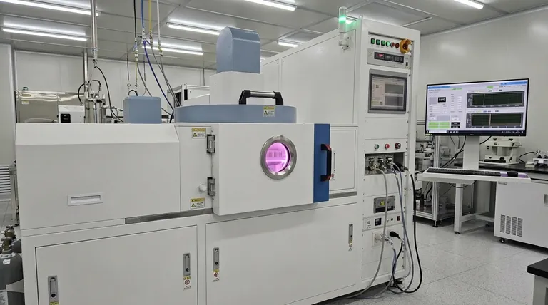
The Core Mechanism: Deposition vs. Sputtering
To understand the advantages of HDP, you must first understand its unique physical process. It operates on a principle of simultaneous deposition and etching.
How Standard Deposition Works
Traditional plasma-enhanced chemical vapor deposition (PECVD) is primarily a deposition-dominant process. Gaseous precursors are energized into a plasma, react, and deposit onto the wafer surface. This process is effective for planar surfaces but struggles with complex topographies.
The HDP Difference: Simultaneous Deposition and Sputtering
HDP, particularly using an inductively coupled plasma (ICP) source, generates a plasma that is orders of magnitude denser than standard PECVD. This creates a high flux of ions directed toward the wafer.
The key is that the HDP process maintains a delicate balance between the rate of deposition from chemical precursors (like silane and oxygen) and the rate of sputtering (physical etching) caused by energetic ions (like Argon).
Advantage 1: Superior Film Quality and Purity
The energetic nature of the HDP process directly contributes to a higher quality film.
Nearly Hydrogen-Free Films
Films deposited from silane (SiH₄) often contain residual hydrogen, which can compromise the dielectric properties and long-term reliability of the device.
The intense ion bombardment in an HDP process is energetic enough to break Si-H bonds and physically knock weakly bonded hydrogen atoms out of the growing film, resulting in a purer, denser silicon dioxide.
Advantage 2: Excellent Conformality and Gap Fill
This is the most significant advantage of HDP-CVD and the primary reason for its use in advanced semiconductor manufacturing.
The Challenge of High-Aspect-Ratio Gaps
As device features shrink, manufacturers must fill extremely narrow and deep trenches (high-aspect-ratio structures) without creating voids or seams. Standard deposition methods tend to "bread-loaf," closing off the top of a trench before the bottom is filled, trapping a void inside.
Sputter-Redistribution for Void-Free Fills
The sputtering component of the HDP process preferentially removes material from angled surfaces, such as the corners at the top of a trench. This sputter-etching rounds the corners, keeping the trench open longer and allowing precursor gases to reach the bottom.
Simultaneously, the sputtered material is redistributed, effectively "plastering" it onto the trench sidewalls and bottom. This combined action ensures the gap is filled from the bottom up, producing a dense, seamless, and void-free fill.
Understanding the Trade-offs
No process is without its compromises. The power of HDP also introduces potential challenges.
Potential for Substrate Damage
The same intense ion bombardment that improves film quality can, if not carefully controlled, cause physical damage to the underlying silicon substrate or other sensitive layers. Process tuning is critical.
Slower Net Deposition Rate
Because the process is constantly etching away a portion of the deposited film, the net deposition rate of HDP is typically lower than that of a deposition-only process like PECVD.
System Complexity and Cost
HDP-CVD systems are more complex and expensive than standard PECVD tools, reflecting the advanced hardware required to generate and control the high-density plasma.
Making the Right Choice for Your Goal
Selecting a deposition method depends entirely on the application's specific geometric and material requirements.
- If your primary focus is filling high-aspect-ratio trenches: HDP-CVD is the industry-standard solution for advanced Inter-Layer Dielectric (ILD) and Shallow Trench Isolation (STI) applications.
- If your primary focus is a simple passivation layer on a flat surface: A faster, lower-cost method like PECVD is often more efficient and perfectly suitable.
- If your primary focus is film quality with a damage-sensitive substrate: You must carefully weigh the superior purity of HDP against the potential for ion-induced damage, possibly opting for a lower-energy HDP process or an alternative chemistry.
Ultimately, HDP-CVD provides a unique tool for solving the geometric challenges posed by modern, scaled device architectures.
Summary Table:
| Advantage | Key Benefit |
|---|---|
| Superior Film Quality | High purity, nearly hydrogen-free, dense films due to intense ion bombardment |
| Excellent Gap Fill | Void-free filling of narrow, high-aspect-ratio trenches via sputter-redistribution |
| Trade-offs | Potential substrate damage, slower deposition rate, higher system complexity |
Unlock the potential of high-density plasma deposition for your semiconductor or advanced material needs with KINTEK! Leveraging exceptional R&D and in-house manufacturing, we provide diverse laboratories with advanced high-temperature furnace solutions, including our CVD/PECVD Systems. Our strong deep customization capability ensures we can precisely meet your unique experimental requirements, delivering superior film quality and gap-fill performance. Contact us today to discuss how our tailored solutions can enhance your research and production efficiency!
Visual Guide

Related Products
- RF PECVD System Radio Frequency Plasma Enhanced Chemical Vapor Deposition
- Slide PECVD Tube Furnace with Liquid Gasifier PECVD Machine
- Inclined Rotary Plasma Enhanced Chemical Deposition PECVD Tube Furnace Machine
- Inclined Rotary Plasma Enhanced Chemical Deposition PECVD Tube Furnace Machine
- Custom Made Versatile CVD Tube Furnace Chemical Vapor Deposition CVD Equipment Machine
People Also Ask
- What gases are used in the PECVD system? Optimize Thin Film Deposition with Precise Gas Selection
- What role does PECVD play in optical coatings? Essential for Low-Temp, High-Precision Film Deposition
- How does plasma vapor deposition work? A Low-Temperature Solution for Advanced Coatings
- What information does laboratory XRD provide for Gallium Sulfide? Master GaS Single Crystal Characterization
- What is PECVD equipment? A Guide to Low-Temperature Thin-Film Deposition

