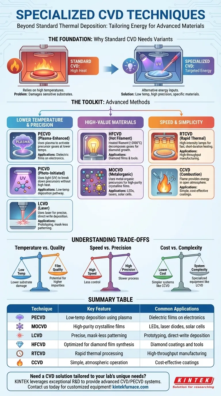
Specialized Chemical Vapor Deposition (CVD) techniques are advanced variations of the standard thermal process, each designed to overcome specific limitations. Methods such as Plasma-Enhanced CVD (PECVD), Metalorganic CVD (MOCVD), and Laser CVD (LCVD) modify how energy is delivered to the precursor gases, enabling deposition at lower temperatures, with higher precision, or for creating highly specific materials like diamond films or compound semiconductors.
The core difference between standard CVD and its specialized variants is not the goal—depositing a thin film—but the method of energy input. By replacing or supplementing generalized heat with plasma, light, or localized heating, these techniques provide precise control over the deposition environment to meet specific application demands.
The Foundation: Why Standard CVD Needs Variants
The Core Principle of CVD
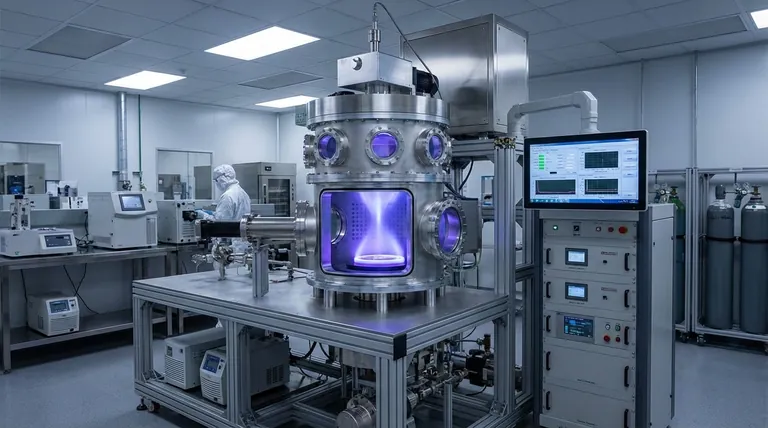
Chemical Vapor Deposition is a process where a substrate is exposed to volatile precursor gases within a reaction chamber. These gases decompose upon activation, typically by heat, and the desired material deposits as a thin, solid film on the substrate surface. This process ensures uniform, complete coverage even on complex shapes.
The Inherent Limitation: High Heat
Standard thermal CVD relies on heating the entire chamber and substrate to high temperatures to initiate the chemical reaction. This works well for robust materials but can damage or destroy sensitive substrates, such as those used in microelectronics or polymers. This single limitation is the primary driver for developing specialized CVD methods.
Specialized CVD: A Toolkit for Advanced Materials
Lowering Temperature with Plasma: PECVD
Plasma-Enhanced CVD (PECVD) uses an electric field to generate a plasma (an ionized gas) in the reaction chamber. This highly energetic plasma activates the precursor gases at much lower temperatures than thermal CVD requires.
This makes PECVD indispensable for depositing dielectric films like silicon nitride and amorphous silicon onto temperature-sensitive integrated circuits.
Using Light for Energy and Precision: PICVD & LCVD
Photo-Initiated CVD (PICVD) utilizes a light source, typically ultraviolet (UV), to break down precursor molecules. The energy from the photons drives the chemical reaction without needing high substrate heat, offering another low-temperature deposition pathway.
Laser CVD (LCVD) takes this a step further by using a highly focused laser beam. The laser can either heat a very small spot on the substrate or directly break down the gas molecules in its path, allowing for precise, direct-write deposition without the need for masks.
Targeting Specific High-Value Materials: HFCVD & MOCVD
Hot Filament CVD (HFCVD) is a technique optimized for synthesizing diamond films. A tungsten or tantalum filament is heated to over 2000°C to decompose precursor gases like methane and hydrogen, creating the specific atomic hydrogen needed for high-quality diamond growth.
Metalorganic CVD (MOCVD) uses metal-organic compounds as precursors. These specialized molecules are crucial for depositing the high-purity, single-crystal films required for compound semiconductors, which are the building blocks of LEDs, laser diodes, and high-efficiency solar cells.
Optimizing for Speed and Simplicity: RTCVD & CCVD
Rapid Thermal CVD (RTCVD) employs high-intensity lamps to heat the substrate very quickly for short periods. This single-wafer processing method reduces the total thermal exposure time, increasing manufacturing throughput.
Combustion CVD (CCVD), also known as flame deposition, is unique in that it often operates in the open atmosphere. Precursors are added to a flame, which provides the energy for decomposition and deposition onto a nearby substrate. It is a simpler, often lower-cost method suitable for certain types of coatings.
Understanding the Trade-offs
Temperature vs. Film Quality
While low-temperature methods like PECVD prevent substrate damage, the resulting films can have different properties than their high-temperature counterparts. For example, PECVD-grown films may contain higher concentrations of hydrogen, affecting their electrical or optical characteristics.
Speed vs. Precision
Techniques designed for speed and simplicity, like Combustion CVD, sacrifice the pristine vacuum environment of other methods. This can lead to lower film purity and less control over thickness and uniformity compared to slower, more controlled processes like MOCVD or PECVD.
Cost and Complexity
Specialized CVD systems add complexity and cost. A PECVD system requires a plasma generator and RF power supplies, while an LCVD system needs an expensive laser and precise optics. This investment is only justified when the benefits—such as low-temperature processing or selective deposition—are critical.
Making the Right Choice for Your Application
Choosing the correct CVD variant requires aligning the technique's strengths with your primary goal.
- If your primary focus is depositing on heat-sensitive substrates like electronics: PECVD or PICVD are your primary candidates due to their low processing temperatures.
- If your primary focus is creating high-purity crystalline films like diamond or compound semiconductors: HFCVD (for diamond) and MOCVD (for optoelectronics) are purpose-built for these demanding tasks.
- If your primary focus is high-throughput manufacturing: RTCVD offers faster processing cycles, while CCVD can provide a simple, scalable atmospheric pressure solution for certain coatings.
- If your primary focus is precise, mask-less patterning for prototyping or repair: LCVD is the ideal choice for its ability to "write" material directly onto a substrate.
Ultimately, selecting the right CVD method is about matching the energy delivery mechanism to your specific material, substrate, and performance requirements.
Summary Table:
| Technique | Key Feature | Common Applications |
|---|---|---|
| PECVD | Low-temperature deposition using plasma | Dielectric films on electronics |
| MOCVD | High-purity crystalline films | LEDs, laser diodes, solar cells |
| LCVD | Precise, mask-less patterning | Prototyping, direct-write deposition |
| HFCVD | Optimized for diamond film synthesis | Diamond coatings and tools |
| RTCVD | Rapid thermal processing | High-throughput manufacturing |
| CCVD | Simple, atmospheric operation | Cost-effective coatings |
Need a CVD solution tailored to your lab's unique needs? KINTEK leverages exceptional R&D and in-house manufacturing to provide advanced high-temperature furnace solutions, including CVD/PECVD systems. Our strong deep customization capability ensures precise matching to your experimental requirements, whether you're working with sensitive substrates or high-value materials. Contact us today to discuss how we can enhance your deposition processes with reliable, customized equipment!
Visual Guide
Related Products
- Custom Made Versatile CVD Tube Furnace Chemical Vapor Deposition CVD Equipment Machine
- Split Chamber CVD Tube Furnace with Vacuum Station CVD Machine
- Multi Heating Zones CVD Tube Furnace Machine for Chemical Vapor Deposition Equipment
- Slide PECVD Tube Furnace with Liquid Gasifier PECVD Machine
- Inclined Rotary Plasma Enhanced Chemical Deposition PECVD Tube Furnace Machine
People Also Ask
- What is a CVD tube furnace and what is its primary function? Discover Precision Thin-Film Deposition
- Why are CVD tube furnace sintering systems indispensable for 2D material research and production? Unlock Atomic-Scale Precision
- How might AI and machine learning enhance CVD tube furnace processes? Boost Quality, Speed, and Safety
- How can integrating CVD tube furnaces with other technologies benefit device fabrication? Unlock Advanced Hybrid Processes
- What are the key application fields of CVD tube furnaces? Unlock Precision in Thin-Film Synthesis


