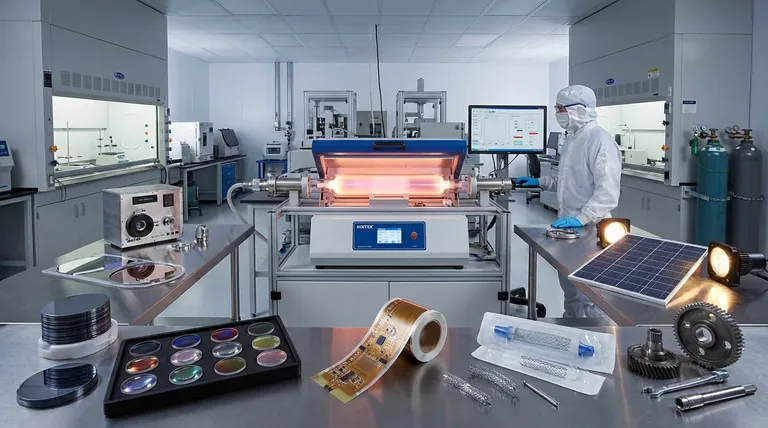
At its core, Plasma-Enhanced Chemical Vapor Deposition (PECVD) is a foundational technology for manufacturing advanced electronics and materials. Its primary applications are in the semiconductor industry for creating integrated circuits, but its use extends broadly to solar cells, optical lenses, protective packaging, and even medical implants. PECVD excels at depositing thin, functional films onto a substrate.
The true value of PECVD is its ability to deposit high-quality functional films at significantly lower temperatures than other methods. This single advantage unlocks the ability to coat temperature-sensitive materials like plastics and complex microchips, making it an indispensable tool across modern high-tech industries.
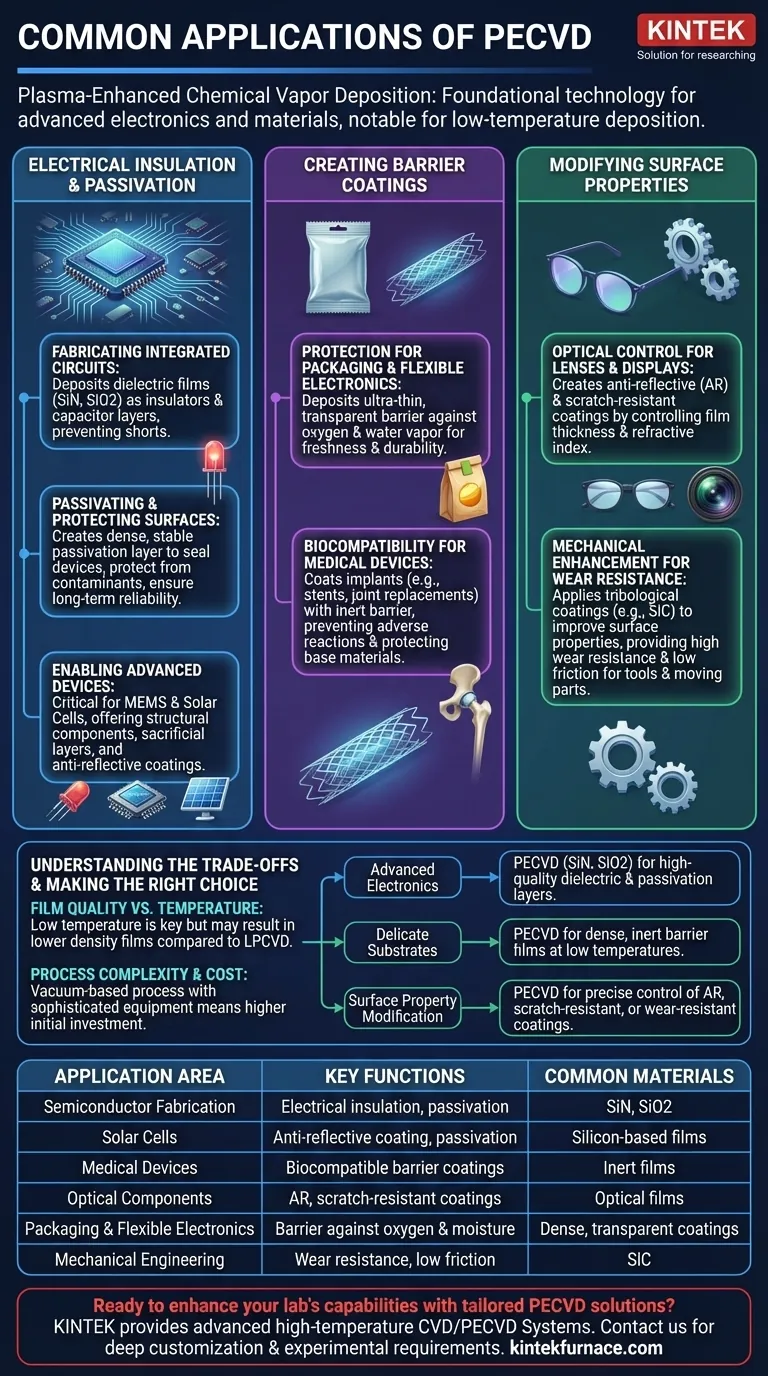
The Role of PECVD in Electrical Insulation and Passivation
The most dominant application of PECVD is in the fabrication of semiconductor devices. Its low-temperature nature is critical for building the complex, multi-layered structures of modern microchips without damaging previously created layers.
Fabricating Integrated Circuits
In an integrated circuit, countless transistors and wires are layered on top of each other. PECVD is used to deposit dielectric films, most commonly silicon nitride (SiN) and silicon dioxide (SiO2).
These films act as high-performance insulators, preventing electrical "short circuits" between the microscopic conductive layers. They are also used to create capacitors, a fundamental electronic component.
Passivating and Protecting Surfaces
Semiconductor surfaces are extremely sensitive to moisture, ions, and other contaminants that can degrade their performance. PECVD deposits a dense, stable passivation layer over the completed device.
This film hermetically seals and protects the delicate circuitry, ensuring long-term reliability and stability. This is also a critical step in manufacturing high-brightness LEDs and solar cells.
Enabling Advanced Devices like MEMS and Solar
The same principles of insulation and protection are vital for other advanced electronics. In solar cells, PECVD films serve as both a passivation layer and an anti-reflective coating to maximize light absorption.
In Micro-Electro-Mechanical Systems (MEMS), these films can act as structural components, sacrificial layers that are later removed, or hard masks to define patterns.
Creating High-Performance Barrier Coatings
The ability of PECVD to create dense, inert films makes it ideal for applications where protection from the environment is paramount.
Protection for Packaging and Flexible Electronics
Many materials, especially flexible polymers, are permeable to oxygen and water vapor. PECVD is used to deposit an ultra-thin, transparent barrier coating that dramatically improves their protective properties.
This is seen in modern food packaging, such as metallic-looking chip bags, where a thin PECVD layer keeps the product fresh. It is also essential for protecting flexible electronic displays from environmental degradation.
Biocompatibility for Medical Devices
When a device is implanted in the human body, it must be biocompatible, meaning it doesn't cause an adverse reaction. PECVD is used to coat medical implants, such as stents or joint replacements.
The deposited film creates an inert barrier that protects the implant from the corrosive environment of the body and, simultaneously, protects the body from the implant's base materials.
Modifying Surface Properties
Beyond electrical and barrier functions, PECVD is used to fundamentally change the mechanical or optical properties of a surface.
Optical Control for Lenses and Displays
By precisely controlling a film's thickness and refractive index, PECVD can create high-performance optical coatings. The most common application is for anti-reflective (AR) coatings on eyeglasses, camera lenses, and solar panels.
It is also used to deposit hard, scratch-resistant coatings on plastic lenses and other optical components, significantly improving their durability.
Mechanical Enhancement for Wear Resistance
In mechanical engineering, PECVD is used to apply tribological coatings—thin films designed to improve surface properties under friction.
These hard coatings, such as silicon carbide (SiC), provide excellent wear resistance and a low coefficient of friction, extending the life of moving parts and tools.
Understanding the Trade-offs of PECVD
While incredibly versatile, PECVD is not the optimal choice for every thin-film application. Understanding its limitations is key to using it effectively.
Film Quality vs. Deposition Temperature
The primary advantage of PECVD is its low processing temperature. However, this comes at a cost. Films deposited at lower temperatures can have lower density and higher hydrogen content compared to those from high-temperature processes like Low-Pressure CVD (LPCVD). For applications demanding the absolute highest film purity and density, a higher-temperature method may be required if the substrate can tolerate it.
Process Complexity and Cost
PECVD is a vacuum-based process that requires sophisticated equipment to generate the plasma and handle reactive gases. This makes the initial capital investment and operational complexity higher than atmospheric pressure techniques. For simple coatings on robust substrates where high quality isn't critical, other methods might be more cost-effective.
Making the Right Choice for Your Goal
The best deposition method depends entirely on the requirements of your specific application and substrate.
- If your primary focus is advanced electronics: PECVD is the industry standard for depositing high-quality dielectric and passivation layers like SiN and SiO2 on sensitive semiconductor wafers.
- If your primary focus is protecting a delicate substrate: Use PECVD for its unique ability to create dense, inert barrier films at low temperatures, making it ideal for polymers, packaging, and medical devices.
- If your primary focus is modifying surface properties: PECVD offers precise control for creating anti-reflective, scratch-resistant, or wear-resistant coatings for optical and mechanical applications.
Ultimately, PECVD's value lies in its unique ability to engineer functional surfaces on a vast array of materials without causing thermal damage.
Summary Table:
| Application Area | Key Functions | Common Materials Deposited |
|---|---|---|
| Semiconductor Fabrication | Electrical insulation, passivation | Silicon nitride (SiN), silicon dioxide (SiO2) |
| Solar Cells | Anti-reflective coating, passivation | Silicon-based films |
| Medical Devices | Biocompatible barrier coatings | Inert films for implants |
| Optical Components | Anti-reflective, scratch-resistant coatings | Optical films with controlled refractive index |
| Packaging & Flexible Electronics | Barrier against oxygen and moisture | Dense, transparent coatings |
| Mechanical Engineering | Wear resistance, low friction | Silicon carbide (SiC) |
Ready to enhance your lab's capabilities with tailored PECVD solutions? Leveraging exceptional R&D and in-house manufacturing, KINTEK provides diverse laboratories with advanced high-temperature furnace solutions, including our specialized CVD/PECVD Systems. Our strong deep customization capability ensures we precisely meet your unique experimental requirements for applications in semiconductors, solar energy, medical devices, and more. Contact us today to discuss how we can support your innovation and efficiency goals!
Visual Guide
Related Products
- Slide PECVD Tube Furnace with Liquid Gasifier PECVD Machine
- RF PECVD System Radio Frequency Plasma Enhanced Chemical Vapor Deposition
- Inclined Rotary Plasma Enhanced Chemical Deposition PECVD Tube Furnace Machine
- Inclined Rotary Plasma Enhanced Chemical Deposition PECVD Tube Furnace Machine
- Multi Heating Zones CVD Tube Furnace Machine for Chemical Vapor Deposition Equipment
People Also Ask
- In which industries is the tube furnace commonly used? Essential for Materials Science, Energy, and More
- What role does a Tube Furnace play in the CVD growth of carbon nanotubes? Achieve High-Purity CNT Synthesis
- What are the disadvantages of tube furnace cracking when processing heavy raw materials? Avoid Costly Downtime and Inefficiency
- What are the typical conditions for plasma-enhanced CVD processes? Achieve Low-Temperature Thin Film Deposition
- How does PECVD equipment contribute to TOPCon bottom cells? Mastering Hydrogenation for Maximum Solar Efficiency


