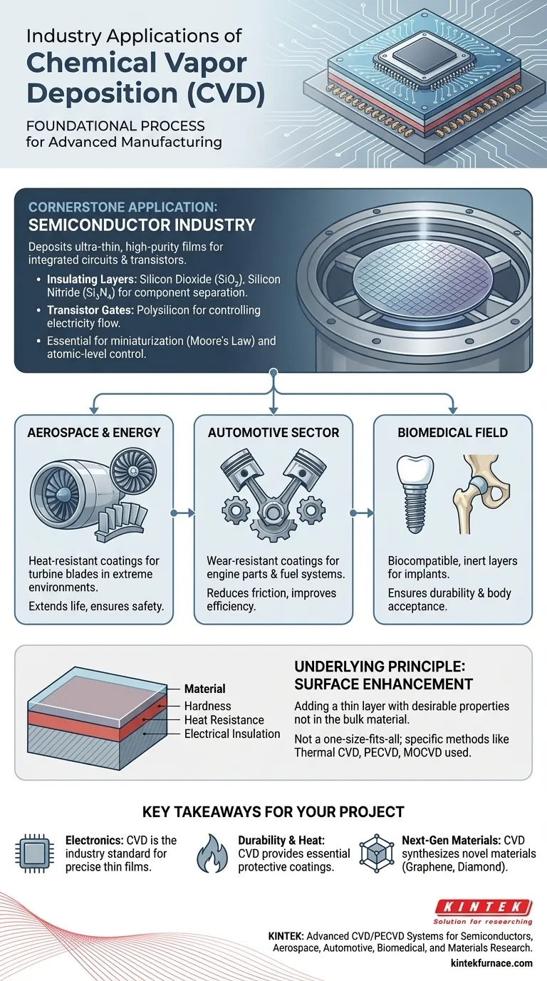
While used across many advanced fields, Chemical Vapor Deposition (CVD) is most frequently and fundamentally employed in the semiconductor industry. Its primary application is the deposition of ultra-thin, high-purity films of materials like silicon dioxide, silicon nitride, and polysilicon, which are the essential building blocks for manufacturing integrated circuits, transistors, and other microelectronic components.
The true power of CVD is not its use in any single industry, but its function as a foundational manufacturing process. It grants engineers the ability to precisely engineer the surface of a material, adding properties like electrical insulation, wear resistance, or heat tolerance that the base material lacks.
The Cornerstone Application: Semiconductor Manufacturing
The modern digital world is built on silicon chips, and CVD is a cornerstone of their fabrication. Without this technique, the complex, layered structures of microprocessors would be impossible to create at a mass scale.
Fabricating Integrated Circuits (ICs)
At its core, an IC is a complex sandwich of insulating, semiconducting, and conducting layers. CVD is the process used to meticulously deposit the insulating layers, such as silicon dioxide (SiO₂) and silicon nitride (Si₃N₄), that separate the millions or billions of components on a single chip, preventing short circuits.
Building Transistors and Diodes
CVD is also used to deposit polysilicon, a key material that acts as the "gate" in a transistor, controlling the flow of electricity. The extreme precision of CVD allows for the creation of these nanometer-scale gates, directly enabling the relentless miniaturization of electronics described by Moore's Law.
Why CVD is Essential Here
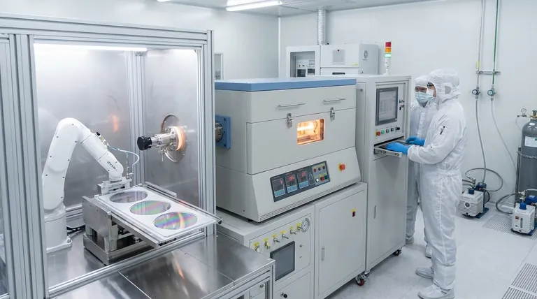
The semiconductor industry demands almost perfect purity and atomic-level control over film thickness. CVD excels by using chemical reactions in a highly controlled vacuum environment, ensuring that the deposited films are uniform, dense, and free from contaminants that would otherwise ruin a microchip.
Beyond Electronics: A Tour of High-Performance Industries
While the semiconductor industry is its largest user, CVD's ability to enhance material surfaces makes it critical in any field where components face extreme conditions.
Aerospace and Energy
In jet engines and power generation turbines, blades operate at incredibly high temperatures in highly corrosive environments. CVD is used to apply hard, heat-resistant coatings to these blades, protecting them from oxidation and wear, thereby extending their life and ensuring operational safety.
Automotive Sector
The automotive industry uses CVD to improve the durability and efficiency of key components. Wear-resistant coatings are applied to engine parts and fuel injection systems to reduce friction and improve longevity, which contributes to better fuel efficiency and lower emissions.
Biomedical Field
For medical implants like artificial hips or dental fixtures, biocompatibility and durability are paramount. CVD is used to apply inert, wear-resistant layers to these implants, ensuring they are not rejected by the body and can withstand decades of mechanical stress.
Advanced Materials Research
CVD is at the forefront of material science innovation. It is a primary method for synthesizing next-generation materials with extraordinary properties, such as graphene, carbon nanotubes, and diamond films, opening doors for new technologies in electronics, energy, and medicine.
Understanding the Underlying Principle
The diverse applications of CVD all stem from a single, powerful capability. Grasping this principle is key to understanding its value.
It's All About Surface Enhancement
The fundamental goal of CVD is to add a thin layer with desirable properties that the bulk material does not possess. A simple steel tool can be transformed into a high-performance cutting instrument by adding a thin, ultra-hard CVD coating. A silicon wafer is transformed into a complex circuit by adding insulating and semiconducting layers.
Not a One-Size-Fits-All Solution
"CVD" is a family of techniques. The specific method—such as Thermal CVD, Plasma-Enhanced CVD (PECVD), or Metalorganic CVD (MOCVD)—is chosen based on the material's heat sensitivity and the desired properties of the final film. For example, PECVD is used for temperature-sensitive materials like those in solar cells.
The Critical Role of Process Control
Achieving a high-quality, durable coating is not automatic. The process requires meticulous optimization of factors like temperature, pressure, gas flow, and how parts are fixtured inside the reactor. Without this control, the resulting film can lack adhesion or fail to provide the intended protection.
How to Apply This to Your Project
Your focus determines how you should view the role of CVD.
- If your primary focus is electronics and microfabrication: CVD is the non-negotiable industry standard for depositing the precise, pure thin films required for functional integrated circuits.
- If your primary focus is mechanical durability and heat resistance: CVD provides essential protective coatings for components in demanding aerospace, automotive, and industrial environments.
- If your primary focus is next-generation material development: CVD is a key enabling technology for synthesizing novel materials like graphene and diamond films from the atomic level up.
Ultimately, Chemical Vapor Deposition is the technology that allows us to build high-performance surfaces, one atomic layer at a time.
Summary Table:
| Industry | Key Applications | Materials Deposited |
|---|---|---|
| Semiconductor | Deposition of insulating layers, transistor gates | Silicon dioxide, silicon nitride, polysilicon |
| Aerospace & Energy | Heat-resistant coatings for turbine blades | Protective coatings (e.g., ceramics) |
| Automotive | Wear-resistant coatings for engine parts | Hard coatings to reduce friction |
| Biomedical | Biocompatible layers for implants | Inert, durable films |
| Advanced Materials | Synthesis of graphene, carbon nanotubes | Novel materials for research |
Ready to enhance your projects with advanced CVD solutions? KINTEK leverages exceptional R&D and in-house manufacturing to provide high-temperature furnace systems like CVD/PECVD Systems, Muffle, Tube, Rotary, Vacuum & Atmosphere Furnaces. Our deep customization capabilities ensure precise solutions for your unique experimental needs in semiconductors, aerospace, automotive, biomedical, and materials research. Contact us today to discuss how we can help you achieve superior surface engineering and material performance!
Visual Guide
Related Products
- Custom Made Versatile CVD Tube Furnace Chemical Vapor Deposition CVD Equipment Machine
- Split Chamber CVD Tube Furnace with Vacuum Station CVD Machine
- Multi Heating Zones CVD Tube Furnace Machine for Chemical Vapor Deposition Equipment
- Slide PECVD Tube Furnace with Liquid Gasifier PECVD Machine
- Controlled Inert Nitrogen Hydrogen Atmosphere Furnace
People Also Ask
- What temperature range do standard CVD tube furnaces operate at? Unlock Precision for Your Material Deposition
- What improvements can be made to the bonding force of gate dielectric films using a CVD tube furnace? Enhance Adhesion for Reliable Devices
- What is a CVD tube furnace and what is its primary function? Discover Precision Thin-Film Deposition
- How can integrating CVD tube furnaces with other technologies benefit device fabrication? Unlock Advanced Hybrid Processes
- Which industries and research fields benefit from CVD tube furnace sintering systems for 2D materials? Unlock Next-Gen Tech Innovations


