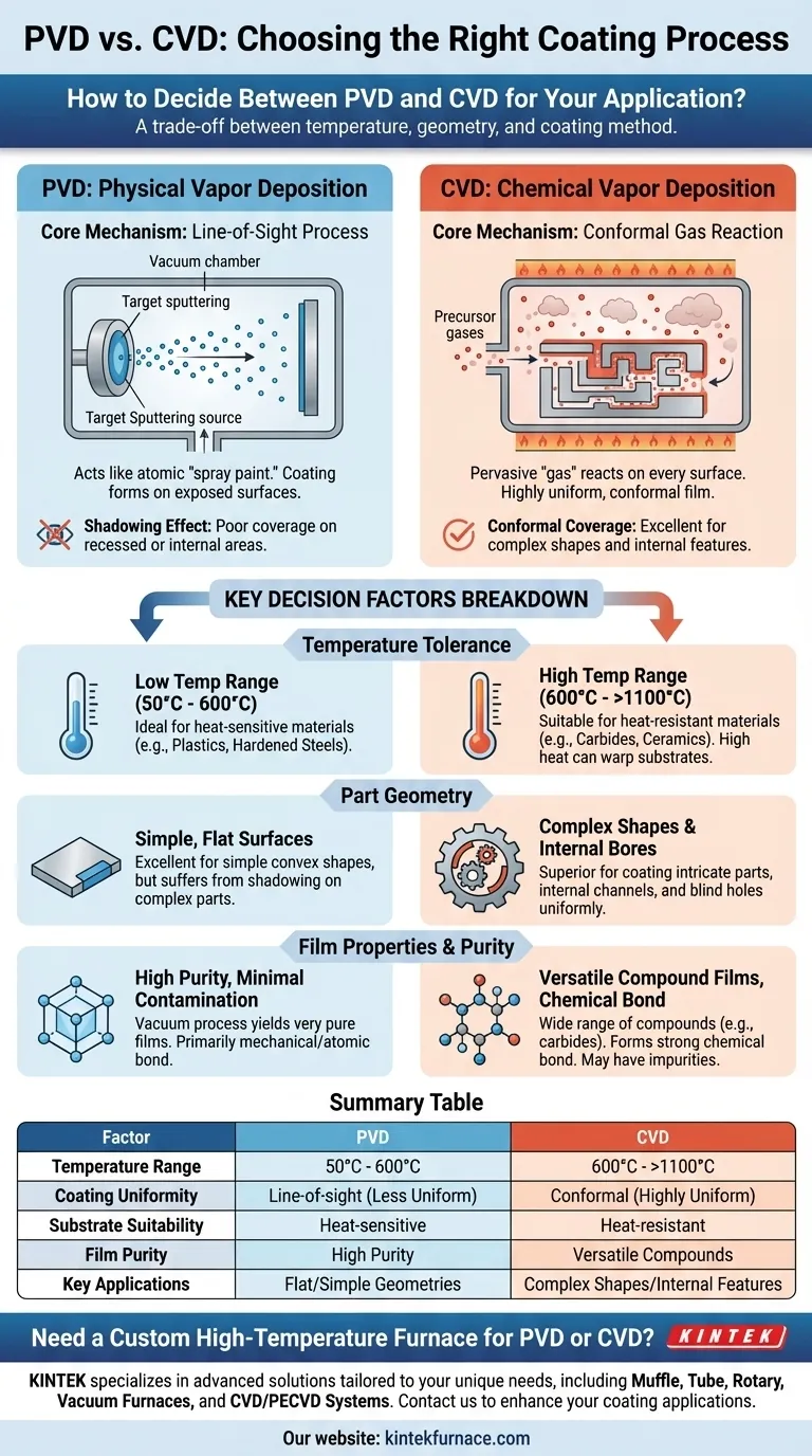
Choosing between PVD and CVD is a critical decision that hinges on a simple trade-off between temperature and geometry. Physical Vapor Deposition (PVD) is a lower-temperature, line-of-sight process ideal for coating heat-sensitive materials. Chemical Vapor Deposition (CVD), while requiring much higher temperatures, excels at creating highly uniform coatings on parts with complex shapes. Your decision will be driven by your material's heat tolerance and the intricacy of the component you need to coat.
The fundamental difference is not the coating itself, but the method of delivery. PVD acts like an atomic "spray paint," coating what it can see, while CVD is a pervasive "gas" that settles and reacts on every exposed surface. Your part's shape and heat sensitivity are the two most important factors in your choice.
The Core Mechanism: Physical vs. Chemical Deposition
To make an informed decision, you must first understand how each process works at a fundamental level. They are not interchangeable; they represent two distinct philosophies of applying a thin film.
How PVD Works: A Line-of-Sight Process
Physical Vapor Deposition (PVD) is a vacuum coating process that operates on a physical principle. A solid source material (the "target") is bombarded with high-energy ions, which knock atoms or molecules loose.
These dislodged particles travel in a straight line through the vacuum chamber and condense onto the substrate (your part), forming a thin film. Think of it as an incredibly precise form of spray painting at the atomic level.
Because the particles travel in a straight line, PVD is a line-of-sight process. Any surface not in the direct path of the source will receive a thinner coating, or none at all.
How CVD Works: A Conformal Gas-Phase Reaction
Chemical Vapor Deposition (CVD) is fundamentally a chemical process. It introduces one or more volatile precursor gases into a reaction chamber containing the heated substrate.
These gases decompose and react on the hot surface of your part, leaving behind the desired solid material as a film. The byproducts of the reaction are then pumped out.
Because the gas flows around and into all features of the part, CVD is a conformal process. It excels at coating all surfaces—including internal bores and complex geometries—with a highly uniform thickness.
Key Decision Factors Breakdown
With the core mechanisms understood, we can evaluate the key factors that will drive your choice for a specific application.
Temperature Tolerance of Your Substrate
This is often the first and most critical filter. PVD processes typically run at relatively low temperatures, often between 50°C and 600°C. This makes PVD suitable for a vast range of materials, including plastics, hardened steels, and finished components that cannot have their properties altered by heat.
CVD, by contrast, is a high-temperature process, frequently requiring temperatures of 600°C to over 1100°C for the chemical reactions to occur efficiently. This heat can anneal, warp, or change the microstructure of the underlying substrate, limiting CVD to materials that can withstand extreme thermal loads, like carbides or certain ceramics.
The Geometry of the Part
The shape of your component is the second major driver. For flat or simple convex surfaces, PVD can provide an excellent, high-quality coating.
For parts with complex shapes, blind holes, or internal channels, CVD is almost always the superior choice. The line-of-sight nature of PVD creates a "shadowing effect," making it very difficult to coat recessed or internal features uniformly without complex part rotation. The precursor gases in CVD, however, can easily penetrate and coat these intricate areas.
Required Film Properties and Purity
PVD is conducted in a high-vacuum environment using a solid, high-purity source material. This inherently results in very high-purity films with minimal contamination.
CVD films can sometimes incorporate impurities from the precursor gases or their chemical byproducts. However, CVD's strength lies in its material versatility, offering a wider range of possible compound films (like silicon carbide or tungsten nitride) that are more easily formed through controlled chemical reactions than through physical deposition.
Understanding the Trade-offs
No process is perfect. Objectively weighing the limitations of each technique is crucial for avoiding costly mistakes.
PVD: The Shadowing Effect and Adhesion
The primary limitation of PVD is its line-of-sight nature. Achieving uniform thickness on complex parts requires sophisticated, and often expensive, fixturing and rotation systems. Even then, perfect uniformity is nearly impossible.
While PVD adhesion is generally strong, the bond is primarily mechanical and atomic. It can sometimes be less robust than the true chemical bond formed during the CVD process.
CVD: Thermal Stress and Chemical Hazards
The high heat of CVD is its greatest weakness. It not only limits the types of substrates you can use but can also introduce thermal stress into the part, potentially causing warping or degradation of mechanical properties.
Furthermore, the precursor gases used in CVD are often toxic, flammable, or corrosive. This necessitates complex safety systems, gas handling equipment, and exhaust treatment, which increases both the capital cost and operational complexity of the system.
Making the Right Choice for Your Application
To make a definitive choice, align the process capabilities with your primary project goal.
- If your primary focus is coating heat-sensitive materials: PVD is the clear choice due to its significantly lower operating temperatures.
- If your primary focus is uniform coverage on complex shapes: CVD's ability to deposit a conformal film makes it the superior option.
- If your primary focus is the highest possible film purity: PVD's vacuum environment and physical sputtering process generally result in fewer contaminants.
- If your primary focus is creating specific compound films (e.g., carbides): CVD offers a more direct and often more effective pathway through controlled chemical reactions.
By understanding the fundamental delivery mechanism—physical line-of-sight versus chemical conformal reaction—you can confidently select the right tool for the job.
Summary Table:
| Factor | PVD | CVD |
|---|---|---|
| Temperature Range | 50°C to 600°C | 600°C to over 1100°C |
| Coating Uniformity | Line-of-sight, less uniform on complex shapes | Conformal, highly uniform on all surfaces |
| Substrate Suitability | Ideal for heat-sensitive materials (e.g., plastics, steels) | Best for heat-resistant materials (e.g., carbides, ceramics) |
| Film Purity | High purity with minimal contamination | Can have impurities, but versatile for compound films |
| Key Applications | Flat surfaces, simple geometries | Complex shapes, internal features |
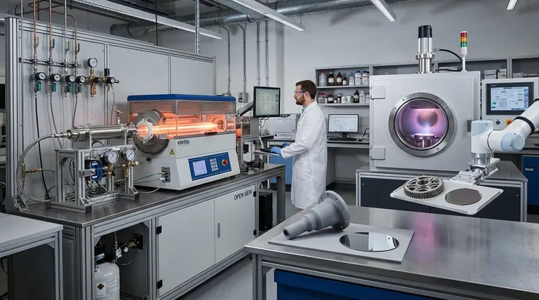
Need a Custom High-Temperature Furnace for Your PVD or CVD Processes?
At KINTEK, we specialize in providing advanced high-temperature furnace solutions tailored to your unique needs. Leveraging exceptional R&D and in-house manufacturing, our product line—including Muffle, Tube, Rotary Furnaces, Vacuum & Atmosphere Furnaces, and CVD/PECVD Systems—ensures precise temperature control and uniform heating for optimal coating results. Whether you're working with heat-sensitive substrates or complex geometries, our deep customization capabilities help you achieve superior performance and efficiency in your laboratory.
Ready to enhance your coating applications? Contact us today to discuss how KINTEK can support your specific requirements!
Visual Guide
Related Products
- HFCVD Machine System Equipment for Drawing Die Nano Diamond Coating
- Custom Made Versatile CVD Tube Furnace Chemical Vapor Deposition CVD Equipment Machine
- Multi Heating Zones CVD Tube Furnace Machine for Chemical Vapor Deposition Equipment
People Also Ask
- What are the equipment for chemical vapor deposition? A Guide to the 5 Essential Components
- What is the significance of the vacuum pressure control system in the CVD coating process for powders?
- What is the function of high-purity Argon (Ar) gas during CVD? Optimize Your Thin Film Uniformity and Purity
- What is the advantage of using a CVD system for coating turbine blades? Master Complex Geometries with Ease
- What core function does CVD equipment serve in h-BN anti-corrosion? Master Precision Synthesis for High-Performance Films


