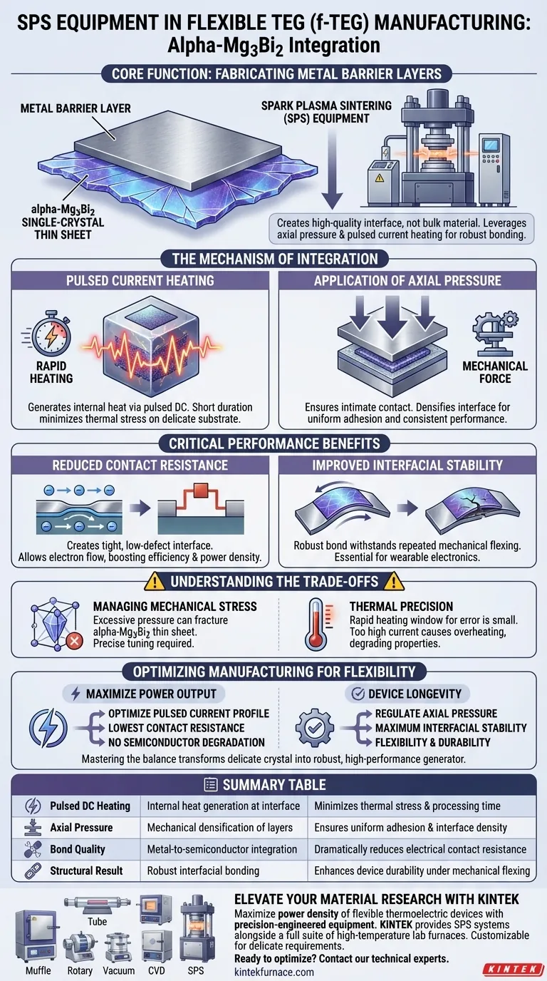
In the realm of flexible thermoelectric generator (f-TEG) manufacturing, Spark Plasma Sintering (SPS) equipment serves a highly specific and critical function: fabricating metal barrier layers directly onto the surfaces of alpha-Mg3Bi2 single-crystal thin sheets. Rather than synthesizing the bulk material itself, the equipment is leveraged to create a high-quality interface between the thermoelectric material and the conductive metal layer.
The core value of SPS in this context lies in its ability to apply axial pressure and pulsed current heating simultaneously. This allows for the rapid formation of a robust bond that significantly reduces contact resistance and enhances interfacial stability, which are prerequisites for high-power density flexible devices.
The Mechanism of Integration
Pulsed Current Heating
SPS distinguishes itself from conventional sintering methods by utilizing pulsed direct current. This generates heat internally within the die and the sample, rather than applying it from an external source.
This method allows for extremely rapid heating rates. Consequently, the metal barrier layer can be bonded to the alpha-Mg3Bi2 substrate in a short duration, minimizing thermal stress on the delicate thin sheet.
Application of Axial Pressure
Simultaneous with the heating, the equipment applies mechanical force. Axial pressure is exerted to ensure intimate contact between the metal barrier material and the thermoelectric sheet.
This pressure is vital for densifying the interface. It ensures that the metal layer adheres uniformly across the surface of the single-crystal sheet, which is essential for consistent electrical performance.
Critical Performance Benefits
Reducing Contact Resistance
The primary technical challenge in f-TEG manufacturing is electrical loss at connections. The SPS process creates a tight, low-defect interface between the metal and the alpha-Mg3Bi2.
This significantly reduces contact resistance. Lower resistance allows electrons to flow more freely across the junction, directly contributing to higher efficiency and power density in the final device.
Improving Interfacial Stability
Flexible devices undergo repeated mechanical stress during use. A weak bond will delaminate or crack, leading to device failure.
SPS achieves a robust bond that creates superior interfacial stability. This ensures the metal barrier remains intact even when the device is subjected to the flexing required of wearable or conformable electronics.
Understanding the Trade-offs
Managing Mechanical Stress
While axial pressure ensures a good bond, it presents a risk to the substrate. Alpha-Mg3Bi2 is utilized here as single-crystal thin sheets, which can be fragile.
Excessive or uneven pressure during the SPS process could fracture the crystal lattice. Process parameters must be tuned precisely to balance sufficient bonding force against the structural limits of the thin sheet.
Thermal Precision
The "short duration" of the process is a benefit, but also a constraint. Because the heating is rapid, the window for error is small.
If the pulsed current is too high, it could cause localized overheating or diffusion of the metal too deep into the thermoelectric material, potentially degrading its thermoelectric properties.
Optimizing Manufacturing for Flexibility
To effectively utilize SPS for alpha-Mg3Bi2 f-TEGs, you must align your processing parameters with your specific device requirements.
- If your primary focus is maximizing power output: Prioritize optimizing the pulsed current profile to achieve the lowest possible contact resistance without degrading the semiconductor.
- If your primary focus is device longevity: Focus on the regulation of axial pressure to ensure a bond that provides maximum interfacial stability against mechanical flexing.
By mastering the balance of pressure and pulsed heat, you transform a delicate single crystal into a robust, high-performance flexible generator.
Summary Table:
| Feature | Function in f-TEG Manufacturing | Key Benefit |
|---|---|---|
| Pulsed DC Heating | Internal heat generation at interface | Minimizes thermal stress & processing time |
| Axial Pressure | Mechanical densification of layers | Ensures uniform adhesion & interface density |
| Bond Quality | Metal-to-semiconductor integration | Dramatically reduces electrical contact resistance |
| Structural Result | Robust interfacial bonding | Enhances device durability under mechanical flexing |
Elevate Your Material Research with KINTEK
Maximize the power density of your flexible thermoelectric devices with precision-engineered equipment. KINTEK provides industry-leading Spark Plasma Sintering (SPS) systems alongside a full suite of Muffle, Tube, Rotary, Vacuum, and CVD systems.
Backed by expert R&D and manufacturing, our high-temperature lab furnaces are fully customizable to meet the delicate pressure and thermal requirements of materials like alpha-Mg3Bi2.
Ready to optimize your manufacturing process? Contact our technical experts today to find the perfect solution for your unique laboratory needs.
Visual Guide
References
- Mingyuan Hu, Jiaqing He. Helical dislocation-driven plasticity and flexible high-performance thermoelectric generator in α-Mg3Bi2 single crystals. DOI: 10.1038/s41467-024-55689-7
This article is also based on technical information from Kintek Furnace Knowledge Base .
Related Products
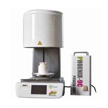
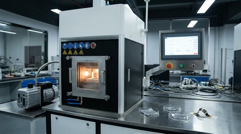
- Spark Plasma Sintering SPS Furnace
- Chairside Dental Porcelain Zirconia Sintering Furnace with Transformer for Ceramic Restorations
- Dental Porcelain Zirconia Sintering Ceramic Vacuum Press Furnace
- 600T Vacuum Induction Hot Press Vacuum Heat Treat and Sintering Furnace
- Vacuum Hot Press Furnace Machine Heated Vacuum Press Tube Furnace
People Also Ask
- What are the steps in the discharge plasma sintering process? Master Fast, High-Density Material Consolidation
- What are the main types of sintering furnaces? Find the Perfect Match for Your Materials
- What is unique about the heating mechanism of a Spark Plasma Sintering (SPS) furnace when preparing nanostructured h-BN ceramics? Achieve Ultra-Fast Densification and Suppress Grain Growth
- Why is it necessary to maintain a high vacuum environment during the SPS of SiC? Key to High-Density Ceramics
- What is the temperature of a sintering furnace? From 1100°C to 2200°C+ for Your Material