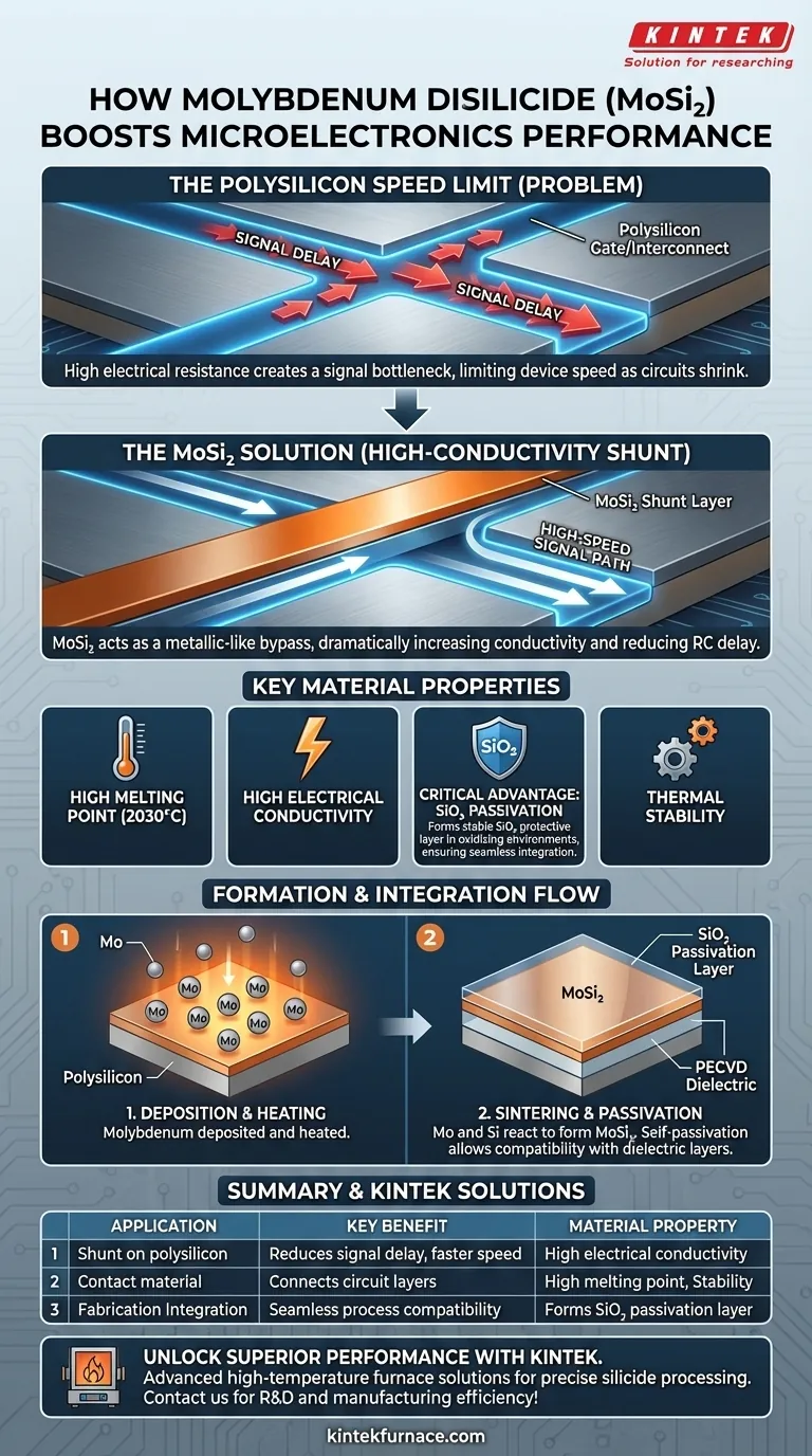
In microelectronics, molybdenum disilicide (MoSi₂) is primarily used as a specialized conducting material layered on top of polysilicon lines. This application, known as a "shunt," dramatically increases the conductivity of these lines, which in turn reduces signal delay and allows for faster device performance. It also serves as a robust contact material for connecting different layers within an integrated circuit.
The core problem in microelectronics is speed. As circuits shrink, the inherent electrical resistance of standard materials like polysilicon creates a signal bottleneck. Molybdenum disilicide acts as a metallic-like bypass, or shunt, that solves this resistance problem without disrupting the fundamental silicon-based manufacturing process.
The Core Problem: The Polysilicon Speed Limit
To understand the role of molybdenum disilicide, you first have to understand the material it enhances: polysilicon.
The Traditional Role of Polysilicon
Polysilicon (polycrystalline silicon) has long been a workhorse material in semiconductor fabrication. It is used to form the "gate" electrode in transistors, the critical component that turns the device on and off.
The Resistance Bottleneck
While effective, polysilicon has relatively high electrical resistance compared to metals. In early integrated circuits, this wasn't a major issue. But as components shrank and signal paths grew longer and thinner, this resistance became a significant bottleneck.
High resistance, combined with capacitance (RC), leads to signal delay. This means it takes longer for signals to travel across the chip, directly limiting the processor's maximum clock speed.
Why Molybdenum Disilicide Is the Solution
Molybdenum disilicide is part of a class of materials called silicides. These compounds are formed between a metal (like molybdenum) and silicon, offering a powerful combination of properties.
As a High-Conductivity Shunt
The primary use of MoSi₂ is as a shunt over polysilicon lines. A thin layer of molybdenum disilicide is deposited on top of the polysilicon gate or interconnect.
Because MoSi₂ is far more conductive than the underlying polysilicon, the majority of the electrical current travels through the silicide layer. This drastically lowers the overall resistance of the line, reducing RC delay and enabling faster signal speeds.
Key Material Properties
Several intrinsic properties make MoSi₂ ideal for this purpose:
- High Melting Point: With a melting point of 2030 °C (3686 °F), it easily withstands the high temperatures required for subsequent steps in chip manufacturing.
- Electrical Conductivity: It is electrically conductive, behaving much like a metal, which is essential for its role as a low-resistance shunt.
- Thermal Stability: It remains stable and does not react undesirably with other materials during high-temperature processing.
The Critical Advantage: SiO₂ Passivation
The most important property of MoSi₂ in a silicon-based process is its behavior at high temperatures. When exposed to an oxidizing environment, it forms a stable, high-quality passivation layer of silicon dioxide (SiO₂) on its surface.
This is a massive advantage. Silicon dioxide is the primary insulator used in microelectronics. Because MoSi₂ naturally forms the same protective material, it integrates seamlessly into standard fabrication flows, preventing oxidation and ensuring compatibility with other process steps like dielectric deposition via PECVD.
Understanding the Trade-offs and Manufacturing
Introducing any new material into a fabrication process requires careful consideration of its formation and potential challenges.
How MoSi₂ Layers Are Formed
Molybdenum disilicide layers are typically created by depositing molybdenum onto the polysilicon and then heating the wafer. This thermal process, or sintering, causes the molybdenum and silicon to react and form the desired silicide compound.
Other methods like plasma spraying can also be used, but these can sometimes lead to the formation of different material phases (like β-MoSi₂) if cooling is too rapid, requiring precise process control.
Process Integration Challenges
While highly compatible, using silicides adds complexity. Engineers must carefully control the thickness, uniformity, and chemical reaction to ensure the resulting layer has the desired low resistance without creating defects. The self-passivating nature of MoSi₂ helps mitigate many of these risks.
Compatibility with Insulating Layers
The ability of MoSi₂ to form a stable silicon dioxide surface makes it perfectly compatible with subsequent deposition of insulating (dielectric) layers. Processes like Plasma-Enhanced Chemical Vapor Deposition (PECVD) are used to deposit silicon nitride or more silicon dioxide to isolate the conductive lines from other parts of the circuit.
Making the Right Choice for Your Goal
While you may not be choosing this material yourself, understanding its purpose provides deep insight into chip design and performance.
- If your primary focus is on chip performance: Recognize that silicide layers like MoSi₂ are a key technology used to reduce signal delay, enabling the higher clock speeds seen in modern electronics.
- If your primary focus is on fabrication processes: Note that the high-temperature stability and self-passivating nature of MoSi₂ are the crucial properties that allow it to be integrated into complex silicon manufacturing workflows.
- If your primary focus is on material science: Appreciate MoSi₂ as an example of a material engineered to solve a specific problem—in this case, providing metal-like conductivity while retaining compatibility with a silicon ecosystem.
Understanding these material-level solutions is fundamental to grasping the innovations that drive the performance of modern electronic devices.
Summary Table:
| Application | Key Benefit | Material Property |
|---|---|---|
| Shunt on polysilicon lines | Reduces signal delay, increases speed | High electrical conductivity |
| Contact material | Connects circuit layers | High melting point (2030°C) |
| Integration in fabrication | Seamless process compatibility | Forms SiO₂ passivation layer |
Unlock superior performance in your microelectronics projects with KINTEK's advanced high-temperature furnace solutions. Our Muffle, Tube, Rotary, Vacuum & Atmosphere Furnaces, and CVD/PECVD Systems, backed by deep customization, ensure precise material processing for silicides like molybdenum disilicide. Contact us today to discuss how we can enhance your R&D and manufacturing efficiency!
Visual Guide
Related Products
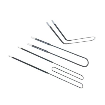
- Molybdenum Disilicide MoSi2 Thermal Heating Elements for Electric Furnace
- Molybdenum Vacuum Heat Treat Furnace
- Vacuum Heat Treat Sintering Furnace Molybdenum Wire Vacuum Sintering Furnace
People Also Ask
- What are the physical properties of MoSi2 heating elements? Unlock High-Temperature Performance
- What are the characteristics of molybdenum disilicide heating elements? Unlock High-Temp Performance
- What are the typical application temperatures for molybdenum disilicide (MoSi2) heating elements? Master High-Temp Performance
- Why are MoSi2 heating elements considered fragile? Understanding Brittleness & Chemical Vulnerability
- What is the primary use of molybdenum disilicide? Ideal for High-Temp Heating Elements